
Professional PCB manufacturing and assembly
Building 6, Zone 3, Yuekang Road,Bao'an District, Shenzhen, China
+86-13410863085Mon.-Sat.08:00-20:00


A High Speed DSP PCB Anti interference Design Technology
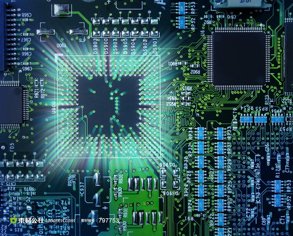
According to the application of printed circuit board, BGA packaging has the characteristics of high success rate, low maintenance rate, high reliability, and is more and more widely used That is, board level design involves many high-speed digital circuit design technologies In high-speed systems, the generation of noise interference is an influencing factor. High frequency circuits will also generate radiation and collisions, while faster edge rates will generate ringing, reflection, and crosstalk If the particularity of high-speed signal layout and wiring is not considered, the designed circuit board will not work properly Therefore, the successful design of PCBis a very critical link in the process of DSP circuit design
1 Transmission line effect
1.1 Signal Integrity
Signal integrity mainly includes reflection, ring tones, ground bounce and crosstalk The locus on the PCB can be equivalent to the series and parallel structures of capacitors. The resistance and inductor are shown in Figure 1 Typical value of series resistance 0.25 days./R-4) 55DJft, parallel resistance is usually very high After adding parasitic resistance, the final impedance of the capacitance and inductance connected to the actual PCB is called the characteristic impedance zo If the impedance of the transmission line and the receiver does not match, this may cause the signal to reflect and oscillate Equivalent circuit of PCB trace: changes in wiring geometry, wrong wiring termination, transmission through connectors, and discontinuities in the power plane will cause reflection When the signal changes at the rising and falling edge of the level, overshoot and undershoot will occur, which will immediately cause small faults higher or lower than the stable level and easily damage the equipment The signal ringing and ringing are caused by improper inductance and capacitance on the line, respectively Ringing can be reduced by proper termination When there is a large current surge in the circuit, it will cause the ground to rebound If a large transient current flows through the power plane of the chip and the circuit board, the parasitic inductance and resistance between the chip package and the power board will cause power noise Crosstalk is a coupling problem between two signal lines. Mutual inductance and capacitance between signal lines will generate noise on the line Capacitive coupling causes coupling current and inductive coupling generates coupling voltage The parameters of the PCB layer, the distance between signal lines, the power characteristics of the driver and receiver, and the wire termination methods all have a certain impact on the crosstalk
Printed circuit board

1.2 Solution
Some measures to be taken to solve common problems: this power plane does not restrict this direction of current flow, the return line can follow the impedance path, that is, close to the signal line This may form a current loop, which will be the development direction of high-speed systems However, the power layer cannot eliminate line clutter. If you do not pay attention to the distribution lines, all systems will generate noise and cause errors Therefore, a special screening program is required, which is realized by bypass capacitor Typically, 1 to 1 Op capacitors F is placed at the power input terminal of the board, and 0 capacitor. 01p. F to U0.1 are placed between the power and ground pins of each active device on the board The bypass capacitor acts like a filter The large capacitor (10aF) is placed at the power input to filter out the low frequency (60Hz) noise generated outside the board. The noise generated by active components on the circuit board is 100MHz or higher The bypass capacitor placed between each chip is usually much smaller than the capacitor placed on the power input terminal of the board According to experience, if analog and digital parts are mixed in the design, the PCB is divided into analog and digital parts. The analog device is placed in the analog part, the digital device is placed in the digital part, and the A/D converter is placed in the entire area Analog signals and digital signals are wired in their respective areas to ensure that the return current of digital signals will not flow into the grounding of analog signals Bypass and decoupling prevent energy from being transferred from one circuit to another Pay attention to the three circuit areas of the power layer, the bottom line layer, components and internal power connections Try to widen the width of power supply and ground wire The ground wire is wider than the power line "-'0.07 mm, power cord 1.2 "-'2.5 n'Lrfl. Use a large area of copper layer as the ground wire, and connect the unused part of the printed board to the ground as the ground wire. Or make a multilayer board, with one layer of power supply and one layer of ground wire respectively. It is equipped with 0. One core ceramic capacitor for each IC chip. If the space of the printed circuit board is too small to install, 1-10 core tantalum electrolytic capacitors can be configured for every 4-10 chips. The high-frequency impedance of the equipment is particularly small, and the impedance is within the range of 500kI-Iz-20MHz. Less than lQ, and the leakage current is very small (below O.5LlA). The decoupling filter capacitor must be installed close to the integrated circuit, and efforts should be made to make the capacitor lead short and the area of the transient current loop small, especially the high-frequency bypass capacitor should not have leads When the system operates at 50MHz, there will be transmission line effect and signal integrity problems, and the traditional measures can achieve satisfactory results; When the system clock reaches 120MHz, it is necessary to consider using high-speed circuit design knowledge Otherwise, on the basis of traditional methods, the PCB designed cannot work normally Therefore, high-speed PCB circuit design has become a design technology that electronic system designers must master
2. PCB high speed signal circuit design technology
2.1 High-speed signal routing
The use of multi layer boards for high speed signal wiring is not only necessary for wiring In order to reduce the size of the PCB, it is necessary to reasonably select the number of layers, make full use of the middle layer to set the mask, and realize the nearest grounding, which can effectively reduce the parasitic inductance, shorten the signal transmission length, and reduce the cross interference between signals, All these are very important for high-speed circuits The reliability of the work is beneficial According to some data, the noise of the four layer board was 20 dB lower than that of the double-sided board when using the same information at the eighth National Anti Radiation Electronic and Electromagnetic Pulse Academic Exchange Conference in 248 The smaller the wire bend, the better Use full straight line, need to turn It can rotate through a 45 degree broken line or circular arc. It can reduce the external emission and mutual coupling of high-speed signals, and reduce the radiation and reflection of signals The lead between pins of high-speed circuit equipment shall be as short as possible The longer the lead, the greater the distributed inductance and capacitance, which will cause reflection and oscillation in high-speed circuit systems It is better to have less lead layer alternation between pins of high-speed circuit components. That is, it is better to use fewer vias during component connection According to the measurement, the through-hole can generate about 0. 5 pF of distributed capacitance, which leads to a significant increase in circuit delay In high-speed circuit wiring, attention should be paid to "cross interference" caused by parallel wiring of adjacent signal lines If parallel distribution cannot be avoided, a large area of "ground" can be arranged on the other side of the parallel signal line to reduce interference On two adjacent layers, the direction of the trajectory must be perpendicular to each other For particularly important signal lines or local devices, measures should be taken to surround the ground wire The protective ground wire can be added around, and it is not easy to interfere with the signal track, such as clock signal and high-speed analog signal. The signal wire to be protected can be clamped in the middle Various signal tracks cannot form a loop, and the grounding wire cannot form a current loop If loop wiring circuit is generated, it will cause great interference to the system The use of daisy chain wiring can effectively avoid loops in the wiring process One or more high-frequency decoupling capacitors shall be placed near each IC block High frequency choke coil, digital ground wire, etc. shall be used for ground wire analogy Connect to common ground Some high-speed signal lines should be specially treated: differential signals should be on the same layer and as close to parallel traces as possible. It is not allowed to insert signals between differential signal lines. Their lengths must be equal Branches or stumps shall be avoided in high-speed signal routing High frequency signal lines are easy to generate large electromagnetic radiation when running on the surface If the high-frequency signal line is routed between the power supply and the grounding wire, the power supply and the bottom layer will absorb electromagnetic waves, which will greatly reduce the radiation generated
2.2 High-speed clock signal routing
Clock circuits play an important role in digital circuits. C64x DSP is a member of C6000 platform and has high processing speed The high-speed clock of C64xDSP can reach 1.1 GHz, which is 10 times higher than that of earlier C62xDSP Therefore, the requirements of clock wiring in the application design of DSP modern electronic system in the future will be higher and higher Priority of high-speed clock signal line Generally, the main clock signal line of the system needs to be given priority when wiring The signal frequency of high-speed clock signal line is high, and the track is required to be as short as possible to ensure signal distortion High frequency clocks are particularly sensitive to noise interference It is necessary to protect and mask the high-frequency clock signal line to reduce interference High frequency clocks (clocks above 20MHz, or clocks with a rising edge of less than 5ns) must be etched by ground wires. The line width of clocks shall be at least 10rail, and the line width of protective ground wires shall be at least 20mil Both ends of the protective ground wire of the high-frequency signal line must be in good contact with the ground through the through hole, and a through hole shall be drilled every 5cm or so to connect with the ground; The length of ground wire escort and data cable is basically the same, and manual wiring is recommended; The clock sending side must be grounded Connect a damping resistor of about 22 to 220Q High speed clock signal tracking design should be designed on the same layer as far as possible, and there should be no other interference sources and tracks around the high-speed clock signal track For high frequency clock connection, star connection or point-to-point connection is recommended When using T-type connection, it is necessary to ensure the same arm length and minimize the number of vias Copper should be used under the crystal oscillator or clock chip to prevent interference Avoid interference caused by signal noise introduced by these lines In high-speed signal wiring and high-speed clock signal wiring, it is required that the opening and branching degree of wiring should be small to avoid stumps, signal reflection and cross windings The influence of vias and stubs at high speed is not only reflected in the influence of PCB on signal, but also leads to the change of wire impedance The influence of via and stub on impedance is often ignored by designers Select a reasonable through hole size For example, for 4-layer to 10 layer PCB design, the common choice is 10mil/20mil (drilling/pad) or 16mil/30mil vias 8 miles/18 mil vias can be used The size of power supply or grounding via can be larger to reduce impedance The power and grounding pins should be placed near the through-hole, and the lead between the through-hole and the pin should be as short as possible At the same time, the power and ground wires should be as thick as possible to reduce impedance The high-density system on chip is packaged in BGA or COB, and the pin spacing is getting smaller and smaller The ball pitch has been reduced to 0.6 mm and will continue to be reduced, making it impossible to use traditional wiring tools to lead out the signal lines of packaged equipment At present, there are two methods to solve this problem: (1) lead the signal line from the lower layer through the via hole under the ball; (2) use extremely thin Routing and free-angle routing Find a lead channel in the ball grid array. For such high-density equipment packaged in BGA or COB, only the wiring method with the minimum width and space can be used Only in this way can we ensure high yield and reliability and meet the requirements of high-speed design


Just upload Gerber files, BOM files and design files, and the KINGFORD team will provide a complete quotation within 24h.