

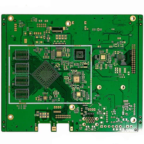
8-layer PCB circuit board
Name: 8-layer PCB circuit board
Layers: 8L
Sheet: FR4 Tg150
Plate thickness: 1.6mm
Panel size: 145*119mm/1
Outer copper thickness: 35μm
Inner layer copper thickness: 35μm
Minimum through hole: 0.20mm
Minimum BGA: 0.35mm
Line width line spacing: 3.8/3.2mil
Surface treatment: Immersion gold 2U''
Application field: face recognition PCB
An 8-layer PCB is a multilayer PCB that provides ample routing space for applications that require multiple power islands. This printed circuit board can help improve EMC performance by adding two planes.
The board is usually mounted on compact devices such as motherboards, wearable watches, backplanes, etc. The increased cost of the 8-layer PCB justifies the increased cost for excellent EMC performance. An 8-layer PCB stackup consists of 4 planes and 4 routing layers connected by 7 rows of dielectric material.
The PCB uses a six-layer board with higher EMC performance. The 8-layer PCB is sealed with solder mask on the bottom and top.
The 8-layer PCB stack-up has many advantages that make it an ideal replacement for other circuit board materials. Following are the advantages of these PCBs;
Minimize fragility: 8-layer PCB reduces device fragility, improving overall performance. This helps shield the inner layer from noise, thereby reducing its vulnerability to external forces.
Reduced Radiation: This type of multi-layer stack helps eliminate any radiation that may occur in high-speed applications. Unlike other stack-ups, the 8-layer PCB eliminates EMI radiation.
Lower operating costs: 8-layer PCB stack-up is a cost-effective option. As for replacement and cleaning, this stack can save you a lot of money. This means that the 8-layer PCB stackup requires low maintenance and is very durable.
Increased functionality: Choosing an 8-layer PCB will help increase the speed and functionality of the device used. Such printed circuit boards are more reliable and practical in different applications. This PCB has more than 4 layers of conductive material to enhance the signal traces.
Application of 8-layer PCB stackup
The 8-layer PCB stackup is the most common type of stackup found in most appliances. This multilayer PCB can be useful in a variety of applications such as:
Medical industry
Automotive industry
Manufacturing
Chemical processing industry
Aviation Industry
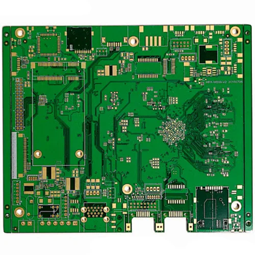
Name: 8-layer PCB circuit board
Layers: 8L
Sheet: FR4 Tg150
Plate thickness: 1.6mm
Panel size: 145*119mm/1
Outer copper thickness: 35μm
Inner layer copper thickness: 35μm
Minimum through hole: 0.20mm
Minimum BGA: 0.35mm
Line width line spacing: 3.8/3.2mil
Surface treatment: Immersion gold 2U''
Application field: face recognition PCB
- Previous: 6-layer industrial control PCB motherboard
- Next:Power Module PWB
