
Professional PCB manufacturing and assembly
Building 6, Zone 3, Yuekang Road,Bao'an District, Shenzhen, China
+86-13410863085Mon.-Sat.08:00-20:00

Copper Deposition Process in PCB Production
Maybe some people who are new to the circuit board factory will wonder that only two sides of the substrate of the circuit board have copper foil, and the middle is the insulating layer. So they don't need to be connected between two or more layers of circuits on the circuit board? How can the circuits on both sides be connected together to make the current flow smoothly?
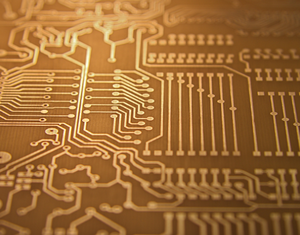
Sunk copper wire
Now let's see the circuit board manufacturer explain the magic process - copper deposition (PTH).
Copper plating is the abbreviation of Electroless Plating Copper, also known as Plated Through hole, abbreviated as PTH, which is a self catalyzed redox reaction. The process of PTH shall be carried out after the drilling of two or more layers of boards is completed.
Function of PTH: chemically deposit a thin layer of chemical copper on the drilled non-conductive hole wall substrate as the base for subsequent copper electroplating.

Decomposition of PTH process: alkaline degreasing → secondary or tertiary countercurrent rinsing → roughening (micro etching) → secondary countercurrent rinsing → pre leaching → activation → secondary countercurrent rinsing → degumming → secondary countercurrent rinsing → copper precipitation → secondary countercurrent rinsing → acid leaching
PTH detailed process explanation:
1. Alkaline degreasing: remove oil stains, fingerprints, oxides, and dust in the hole; The hole wall is adjusted from negative charge to positive charge, which is convenient for the adsorption of colloidal palladium in the subsequent process; Cleaning after oil removal shall be carried out in strict accordance with the requirements of the guidelines and shall be tested by copper sinking backlight test.
2. Micro etching: remove the oxide on the board surface, coarsen the board surface, and ensure a good adhesion between the subsequent copper deposition layer and the base copper; The newly formed copper surface has strong activity and can well adsorb colloidal palladium;
3. Pre leaching: It is mainly to protect the palladium tank from the pollution of pre-treatment tank liquid, and extend the service life of the palladium tank. The main components are consistent with those of the palladium tank except palladium chloride, which can effectively wet the hole wall, so that subsequent activation liquid can enter the hole in time for sufficient and effective activation;
4. Activation: after the adjustment of the polarity of alkaline oil removal by pretreatment, the positively charged pore wall can effectively absorb enough negatively charged colloidal palladium particles to ensure the average, continuity and compactness of subsequent copper deposition; Therefore, oil removal and activation are crucial to the quality of subsequent copper deposition. Key control points: specified time; Standard stannous ion and chloride ion concentration; The specific gravity, acidity and temperature are also very important, which should be strictly controlled according to the operation instructions.
5. Degumming: remove the stannous ions wrapped outside the colloidal palladium particles, expose the palladium core in the colloidal particles, and directly and effectively catalyze the chemical copper precipitation reaction. Experience shows that it is a better choice to use fluoroboric acid as the degumming agent.
6. Copper precipitation: the autocatalytic reaction of chemical copper precipitation is induced by the activation of palladium core. Both the new chemical copper and the reaction by-product hydrogen can be used as the reaction catalyst to catalyze the reaction, so that the copper precipitation reaction continues. After being treated by this step, a layer of chemical copper can be deposited on the plate surface or hole wall. During the process, the tank liquid shall be stirred with normal air to convert more soluble copper.
The quality of the copper sinking process is directly related to the quality of the production PCB, which is only important for the PCB manufacturer. It is the main source process of blocked vias and poor open and short circuits, and it is not convenient for visual inspection. The subsequent process can only be probability screened through destructive experiments, and can not effectively analyze and monitor a single PCB. Therefore, once problems occur, they must be batch problems, Even if the test cannot be completed and eliminated, the final product will cause great potential quality problems and can only be scrapped in batches, so it is necessary to strictly follow the parameters of the operation instructions.
The above is the explanation given by the editor of pcb circuit board company. If you want to know more about PCBA, you can go to our company's home page to learn about it. In addition, our company also sells various circuit boards,
High frequency circuit board and SMT chip are waiting for your presence again.
Why should there be test points on PCB?
Oct 24,2022


Just upload Gerber files, BOM files and design files, and the KINGFORD team will provide a complete quotation within 24h.