
Professional PCB manufacturing and assembly
Building 6, Zone 3, Yuekang Road,Bao'an District, Shenzhen, China
+86-13410863085Mon.-Sat.08:00-20:00

About the Function of PCBThrough Hole and Metal Edge
PCB, the full name of printed circuit board, is the bridge of signal communication between high-tech, including the industrial control board connecting switches and machinery. During the production process of PCB, PCB manufacturers always put a circle of through-hole and copper tape around the industrial control board or RF board. Some RF boards even carry out metallized edging around the board. Many small partners do not understand why they should do this. Could it be that engineers are showing technology, Do useless work?
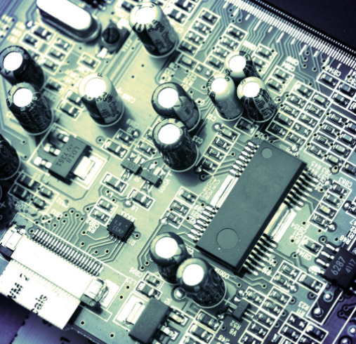
Pcb circuit board

Actually, it is not. It is purposeful. Nowadays, with the improvement of system speed, not only the timing and signal integrity problems of high-speed signals are prominent, but also the EMC problems caused by the electromagnetic interference and power integrity of high-speed digital signals in the system are very prominent. The electromagnetic interference generated by high-speed digital signals will not only cause serious mutual interference within the system, reduce the anti-interference capability of the system, but also generate strong electromagnetic radiation in the outer space, causing the electromagnetic radiation emission of the system to seriously exceed the EMC standard, making the products of circuit board manufacturers unable to pass the EMC standard certification. The edge radiation of multilayer PCB is a common electromagnetic radiation source. When the unexpected current reaches the edge of the ground plane and the power plane, the edge radiation will occur, which is characterized by the grounding and power noise caused by insufficient power bypass. The cylindrical radiation magnetic field generated by the inductive via radiates between layers of the circuit board and finally meets at the edge of the circuit board. The return current of the stripline carrying the high-frequency signal is too close to the edge of the circuit board. In order to prevent these situations, a circle of grounding vias is punched around the PCB at a distance of 1/20 wavelength holes to form a grounding vias shield to prevent external radiation of TME waves.
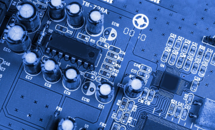
Pcb board
For microwave circuit boards, the wavelength is further reduced. Because of the current PCB production process, the spacing between holes cannot be very small. At this time, the way that 1/20 of the wavelength spacing is used to drill shielding vias around the PCB has no obvious effect on microwave boards. At this time, it is necessary to use the PCB version metallized edge wrapping process to surround the entire board edge with metal, so that microwave signals cannot be radiated from the PCB edge. Of course, The use of metal edge bonding process will also lead to a lot of increase in PCB manufacturing costs. For RF microwave boards, some sensitive circuits, and circuits with strong radiation sources, a shielding cavity welded on the PCB can be designed. When designing a PCB, a "through hole shielding wall" should be added, that is, a grounded through hole should be added at the position close to the shielding cavity wall on the PCB. In this way, relatively isolated areas are formed. After confirmation, it can be sent to the multilayer circuit board manufacturer for production.
The above is the explanation given by the editor of pcb circuit board company. If you want to know more about PCBA, you can go to our company's home page to learn about it. In addition, our company also sells various circuit boards,
High frequency circuit board and SMT chip are waiting for your presence again.
How to avoid finger print on PCB?
Oct 24,2022


Just upload Gerber files, BOM files and design files, and the KINGFORD team will provide a complete quotation within 24h.