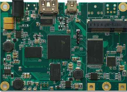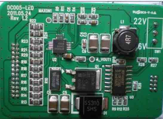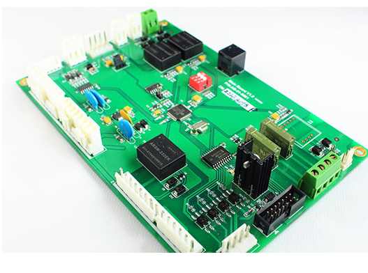
OSP is an organic welding film, also known as copper protection agent, which is mainly to protect copper exposed to the air, which is a common surface treatment process in PCB processing. Nothing is perfect, and OSP is no exception,
OSP acts as a barrier between copper and air, which is different from other surface treatment processes, OSP is organic, not metal, so it is cheaper than the tin spray process. The principle is to grow a layer of organic film on the clean bare copper surface by chemical method, and many computer motherboards use the OSP process.
This layer of organic film can make the circuit board before welding to ensure that the inner layer of copper foil will not be oxidized, welding, once heated, this layer of film will evaporate, solder can solder the copper wire and components together.With all the advantages of bare copper plate welding, expired plates can also be re-finished.
Disadvantages:
1, OSP transparent colorless, more difficult to check, it is difficult to distinguish whether the OSP processing.
2, the OSP itself is insulated, non-conductive, will affect the electrical test. In this way, the test point must open the steel mesh and print the solder paste to remove the original OSP layer, and then contact the needle point for electrical testing. OSP cannot be used as an electrical contact surface, such as a keyboard surface for keys.
3, OSP is not corrosion resistant, easy to be affected by acid and temperature. When used in secondary reflow welding, it needs to be completed within a certain time, usually the second reflow welding effect will be relatively poor. If the storage time exceeds three months, it must be resurfaced and used within 24 hours after opening the package.

An OSP circuit board, exposed to the air for more than ten days, will not be able to weld components. Energy production from 2 layers to 14 layers, 14-22 layers can be proofing production.
Minimum line width/spacing: 3mil/3milBG Distance :0.20MM Minimum aperture: 0.1m Size :610mmX1200mm
Ink: Japan Tamura, Taiyo, Fudoken;
FR4: Shengyi, Kingboard, Haigang, Hongren, Guoji, Hezheng, Nanya, (S1130/S1141/S1170),Tg130℃/ Tg170℃ T g180℃ and other high TG plates)
High frequency board: Rogers, Taconic, ARLLON; Surface process: spray tin, lead-free spray tin, sinking gold, full plate gold plating, plug gold plating, full plate thick gold, chemical sinking tin (silver), anti-oxidation (OSP) blue glue, carbon oil
kinhford Electronics is a circuit board manufacturer specializing in printed circuit board manufacturing, 20 years of focus on single, double sided, multi-layer circuit board production. Can provide FR4 hard board, FPC soft board, HDI board, metal substrate PCB proofing and mass production services.


