
Professional PCB manufacturing and assembly
Building 6, Zone 3, Yuekang Road,Bao'an District, Shenzhen, China
+86-13410863085Mon.-Sat.08:00-20:00


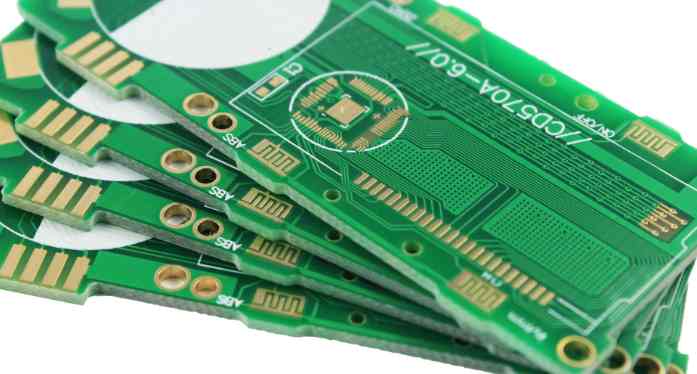
In recent years, the typical processes for manufacturing double-sided circuit boards are SMOBC method and graphic electroplating method. The process wire method is also used in some specific situations.
1.Graphic plating process flow
Covering foil plate → cutting material → punching reference hole → NC drilling → Inspection → Deburring → electroless plating copper → electroplating copper → Inspection → Brush plate → Film coating (or screen printing)→ exposure development (or curing)→ inspection retouching plate → Graphic plating (Cu+Sn/Pb)→ Removing film → etching → Inspection retouching plate → nickel plating on plug → hot melt cleaning → electrical on-off test --> Cleaning process → Screen print solder resistance pattern → curing → screen print mark symbol → curing → shape processing → cleaning and drying → Inspection → packaging → finished product.
In the process, the two processes of "electroless thin copper → electroplated thin copper" can be replaced by a process of "electroless thick copper", both of which have advantages and disadvantages. Graphic electroplating - etching method of double face metallized plate is a typical process in the 1960s and 1970s. In the 1980s, the bare copper covered welding film process (SMOBC) gradually developed, especially in the precision dual panel manufacturing has become the mainstream process.
Two, SMOBC process
The main advantage of SMOBC board is to solve the short circuit phenomenon of solder bridging between thin lines, and because of the constant ratio of lead to tin, it has better weldability and storage than hot melt board. There are many ways to manufacture SMOBC plate, including the SMOBC process of standard pattern electroplating minus method and then removing lead tin; Subtracting pattern electroplating SMOBC process with tin plating or dipping instead of electroplating lead tin; SMOBC process by blocking or masking holes; Addition method SMOBC process, etc.

The following mainly introduces the SMOBC process and the SMOBC process flow of the graphic electroplating method and the plugging method.
1. SMOBC process method for removing lead tin by graphic electroplating:
The SMOBC process for reremoving lead tin by graphic plating is similar to the process of graphic plating. It only changes after etching.
Double-sided copper foil plate → patterned plating process to etching process → lead tin removal → Inspection → Cleaning → Solder resistance pattern → plug nickel plating → plug tape → hot air smoothing → Cleaning → Screen mark symbol → Shape processing → Cleaning and drying → Finished product inspection → packaging → finished product.
2. The main process of plugging method is as follows:
Double-sided foil plate → drilling → electroless copper plating → Whole plate copper plating → Hole blocking → screen printing imaging (positive)→ Etching → removing screen printing material and hole blocking material → Cleaning → solder resistance pattern → plug nickel plating and gold plating → Plug tape → hot air smoothing → the following process is the same as above to the finished product.
The process steps of this process are relatively simple, and the key is to plug the hole and wash the ink of plugging the hole.
In the plugging process, if the plugging ink is not used to plug holes and screen printing imaging, and a special masking type dry film is used to cover the holes, and then exposed to make positive graphics, this is the masking hole process. Compared with the plugging method, it no longer has the problem of cleaning ink in the hole, but it has higher requirements for masking dry film.
SMOBC process is based on the production of bare copper hole metallized double panels, and then the application of hot air leveling process.
PCB single-sided circuit board pad off causes and solutions
There are two reasons for the single-sided circuit board pad to fall off. One is that the thin copper foil is easy to fall off the circuit board pad when the electric soldering iron is used for welding. The other reason is that the copper foil adhesion of the circuit board is secondary, which is easy to cause the pad to fall off during welding.
Once the pad falls off when the circuit board is welding components, the circuit board cannot be used. How can you make the pad not easy to fall off? First of all, do not choose to use soldering iron welding using soldering pot welding or wave welding, these two welding methods are not easy to make the pad fall off and increase the speed of welding, soldering pot can be repaired with soldering iron after soldering. The second method is to let the designer of the circuit board factory beside a piece of copper foil around the circuit board pad, the attachment area is large, the pad is not easy to fall off, if there is no space around the pad beside the copper foil, then the thickness of the copper foil can be increased, the thickness of the copper foil increases in the soldering iron continuous motor can protect the pad.


Just upload Gerber files, BOM files and design files, and the KINGFORD team will provide a complete quotation within 24h.