
Professional PCB manufacturing and assembly
Building 6, Zone 3, Yuekang Road,Bao'an District, Shenzhen, China
+86-13410863085Mon.-Sat.08:00-20:00

What materials do you need to prepare for PCB design?
For board design, the preparation of sufficient information can greatly reduce the error and duplication of work in the development process.
1. Device list The device list lists all the components in the circuit board and their models, quantities, and positions. With an accurate device list, developers can understand the type and specifications of the devices to be used before the PCB design and ensure that they match the rest of the board.
2. Circuit schematic diagram Circuit schematic diagram describes the connection relationship between the various parts of the circuit board and the connection mode of the components. Before the PCB design, the circuit schematic can simulate the working mode of the circuit, find problems and adjust.
3. PCB size and positioning hole position
Since the circuit board needs to be installed inside the device, the PCB size and positioning hole position are very important. If this information is incorrect, the board may not be installed and used. Before PCB design, we need to understand the actual size of the equipment and the space required by the PCB to ensure that the size of the PCB and the location of the positioning hole are correct.
4. PCB layer
PCB layer refers to the distribution of each layer on the circuit board. PCBS typically have a limited number of layers of two to four, including the top, bottom and inner layers. Before PCB design, we need to determine the PCB layer used and the function of each layer.") https://www.kingfordpcb.com/yuan.php?time=1685694568
https://www.kingfordpcb.com/yuan.php?time=1685694568
5. Impedance control parameters
The impedance control parameter describes the impedance value of the circuit transmission line on the PCB. The precise setting of impedance control parameters ensures the performance and characteristics required by the circuit. In the PCB design process, we need to analyze and calculate the physical size and material of the transmission line, and design the impedance control parameters that meet the requirements.
6. Relevant certification documents
The circuit board needs to pass the relevant certification before it can be used normally. In the design process, we need to understand the certification standards and requirements related to the circuit board, and prepare the relevant certification documents and test reports.
7. PCB shell and specifications The circuit board needs to cooperate with other equipment, so the PCB shell and specifications need to be designed according to the actual situation of the equipment. Before PCB design, we need to understand the working environment, working temperature, anti-noise ability and EMC certification requirements of the equipment, and design the corresponding shell and specifications of the PCB.
In short, it is very important to prepare sufficient information before PCB design, which can help us avoid wasting time and resources, and ensure high quality and high performance of PCB.
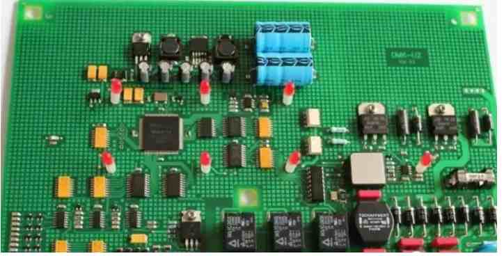
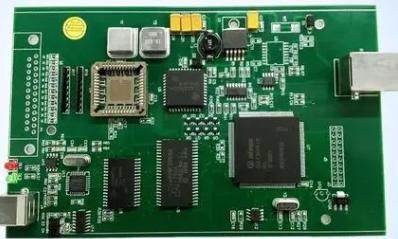
PCBA functional testing is carried out to ensure the electrical performance and functional stability of the product. In the production process, the use of reliable PCBA functional testing can detect defects and faults of the circuit board early, which ultimately improves the quality and reliability of the product. At the same time, through PCBA functional testing, the stability of the product can be guaranteed, thus ensuring subsequent customer satisfaction and credibility.
In PCBA functional testing, a series of testing methods and tools are usually used. The following are common test methods:
1. Point test:
Point test is a traditional circuit board test method. The method requires a set of metal pins or sensors to detect connectivity and insulation on the circuit board. In it, the tester uses a computer program to control the movement of these needles or sensors to test the functions of the PCBA.
2. Flying needle test:
Flying needle test is an automated test method that can test multiple boards simultaneously. The method uses a robotic arm or other machine device to accurately locate and measure the electrical properties of the circuit board. By this method, the testing efficiency of PCBA can be improved.
3. Boundary Scan test:
Boundary scan testing uses a special test rack built into the chip for board testing of external interfaces. This method is particularly suitable for testing complex circuit boards, such as those used for communication or automatic control.
4. Surface Mount (SMT) test:
Surface mount testing can effectively test surface-mount components on the circuit board, such as chips, capacitors, resistors, etc. In addition, when performing surface mount tests, it is also possible to check whether the solder joints on the circuit board are intact.
5. Functional test: Functional testing is one of the most commonly used circuit board testing methods. The method is to verify the normal functions of the circuit board by simulating the operation of the circuit board in actual use conditions. For example, the function test of a PCBA-based TV set includes the TV on, off, volume control, channel control, and so on.
In summary, these are the common PCBA functional testing methods, each of which has its own unique advantages and disadvantages. During PCBA functional testing, appropriate testing methods should be adopted according to the actual situation, and adjustments and improvements should be made according to the test results.


Just upload Gerber files, BOM files and design files, and the KINGFORD team will provide a complete quotation within 24h.