
Professional PCB manufacturing and assembly
Building 6, Zone 3, Yuekang Road,Bao'an District, Shenzhen, China
+86-13410863085Mon.-Sat.08:00-20:00

PCBA: How to design the best printed circuit board assembly
There is a well-known correlation between strength and speed in sports. Basically, strength or power is the determinant of how fast you move. At some point, however, the positive correlation between strength (which is closely related to muscle size) and speed no longer exists, and increasing size and strength actually slows you down. Similarly, in the not too distant past, productivity and efficiency had a comparable relationship in manufacturing.
Today, state-of-the-art manufacturing facilities are highly automated. Reduced reliance on human repetition improves efficiency and productivity, and aligns these metrics more closely with process speed. It is true that the best printed circuit board component (PCBA) device capabilities and process techniques determine productivity and efficiency. Ensuring that the board is properly designed and follows well-assembled design (DFA) guidelines minimizes the need for human intervention. Let's review the process to help identify areas of design focus to maximize PCBA speed.
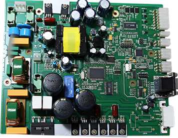
Transforming your design into a complete physical structure requires three steps: 1) manufacturing, 2) component procurement and 3) assembly. Printed circuit board assembly or PCBA is one of two PCB manufacturing processes. The other stage is manufacturing, which starts with execution. During the manufacturing process, your board design is completed and ready for assembly, where the components are securely attached to the board. Although PCBA may consist of ten or more steps, the process can be divided into the following main tasks:")
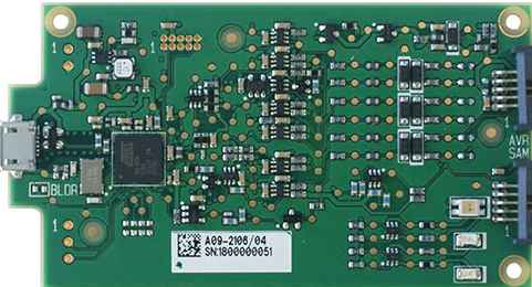
The initial solder paste layer is applied to the pad of the board prior to placing the Surface Mount Technology (SMT) assembly. This is done to promote good flow during welding and minimize assembly defects. The coating method can be manual or automated using template printing or jet printing.
For SMT components, accurate placement of components on pads is critical. Improper alignment may result in poor solder joints or tombstones falling off, where one side of the assembly is not attached to the plate. Through-hole technology (THT) components are more flexible; However, it is generally recommended that the body of the component be as close to the board surface as possible.
The most common method of securing SMT components is reflow soldering. For THT components, wave soldering is the preferred method. If both types of components are used, the SMT component is usually placed and welded first. Only then is the THT component placed and welded, which extends the welding task. The soldering of the two-sided circuit board is further extended because the components are mounted on both top and bottom surfaces. After the welding steps for each component type are completed, the connections are inspected and if any problems are found, rework is required to correct them.
Clean the circuit board https://www.kingfordpcb.com/yuan.phpto remove all excess debris from the surface. Alcohol or deionized water can effectively remove most contaminants.
Split-board is the work of dividing multi-board panels into individual units or PCBS, which is the ultimate primary task and should not be overlooked. Panelization or inefficient panel design can lead to significant waste and additional costs.
The above tasks are performed by your contract manufacturer (CM) and the quality of the manufacturing process depends on your choice of manufacturing and assembly services. However, certain design strategies can be used to optimize PCbas, especially in terms of speed.
Any design decision made with the goal of improving the PCBA can and should be part of the DFA guidelines. These include options designed to improve process efficiency, quality, or speed. In particular, to speed things up, we can define a list of specific tasks that, if executed during the design process, can optimize the process.
PCB assembly speed optimization list planning stage priority speed selection CM and assembly service. Procurement selection components are available throughout the development process. Eliminate or minimize the use of through-hole components. The schematic phase ensures that your component footprints match the BOM exactly. The layout level clearly marks the orientation of components and connectors. Use cooling devices in flat connections. Layout a Panel designed to minimize waste and score where possible for quick, easy separation. Use CM's default material, solder resistance and screen printing color and surface finish. Make sure your design package is complete and accurate, including BOM, engineering drawings and any special information, and is in the best format for CM.
Overview of PCB assembly documentation
Jun 03,2023


Just upload Gerber files, BOM files and design files, and the KINGFORD team will provide a complete quotation within 24h.