
Professional PCB manufacturing and assembly
Building 6, Zone 3, Yuekang Road,Bao'an District, Shenzhen, China
+86-13410863085Mon.-Sat.08:00-20:00

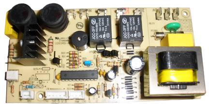
Placement of SMT components on PCB
Each SMT component on the PCB board is placed at a specific location on the conductive path, so that that particular component can receive enough power to function. Special attention is required when considering placing components on printed circuit boards (PCBS) that use surface mount techniques.
Precautions for CTE
Many factors must be considered when establishing SMT component placement tolerances and spacing. One of the most important factors regarding the spacing and placement of SMT components is the coefficient of thermal expansion or CTE. Many printed circuit boards are made of glass epoxy substrates with lead-free ceramic chip carriers. When the CTE gap between them is too large, the phenomenon of solder joint cracking may occur, but it generally occurs after 100 cycles. To avoid this, use a compatible top substrate and ensure adequate thermal expansion, or alternatively use lead-based ceramic chip carriers instead of lead-free ceramic chip carriers.
Where your SMT components are placed also depends on size and cost. Components that absorb more than 10mW or conduct more than 10ma will require more thermal and electrical considerations. Your power management component will need a ground plane or power plane to control heat flow. High current connections will depend on the acceptable voltage drop of the connection. For layer conversion, the high current path requires two to four through-holes at each layer conversion. Placing multiple through-holes at layer transitions increases thermal conductivity, improves reliability and reduces resistance and inductance losses.") https://www.kingfordpcb.com/yuan.php
https://www.kingfordpcb.com/yuan.php
When SMT components are placed, connectors are placed first, followed by power circuits, sensitive and precision circuits, critical circuit components, and any other required components. You are selecting route priorities based on power level, noise sensitivity, and generation and routing capabilities. The number of layers you include will vary depending on the power level and complexity of the design. Keep in mind that since copper cladding is produced in pairs, layers should also be added in pairs.
After placing components, check the layout and make necessary adjustments to the physical location or wiring path. Final considerations should include ensuring that there is a solderproof layer between pins and through holes, that the screen printing is concise and that sensitive circuits and nodes are protected from noise sources. During the audit process, you can make corrections to the PCB based on any feedback you get from the PCB designer.
Placement of SMT conductive components on PCB
Jun 02,2023


Just upload Gerber files, BOM files and design files, and the KINGFORD team will provide a complete quotation within 24h.