
Professional PCB manufacturing and assembly
Building 6, Zone 3, Yuekang Road,Bao'an District, Shenzhen, China
+86-13410863085Mon.-Sat.08:00-20:00

Where can PCBA processing be done
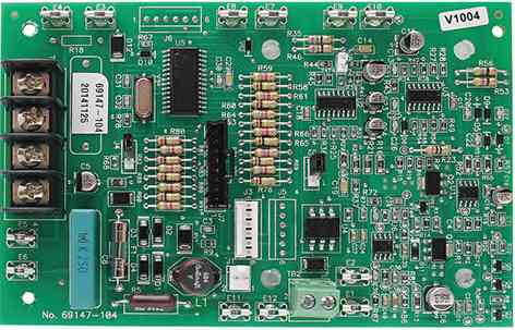
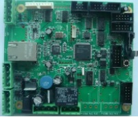
Where can PCBA processing be done? kinhford is a professional PCBA processing manufacturer with more than 20 years of PCBA processing experience. It has its own PCB board factory and SMT patch processing factory, equipped with professional component purchasing specialists and incoming material analysis and control engineers, and can provide PCBA processing and OEM services for electronic products such as industrial control, security, small household appliances and smart home.
1. Make SMT production process documents and generate SMT coordinate documents according to customer Gerber documents and BOM documents;
2. Check whether all production materials are ready, make a complete set of orders, and confirm the PMC plan of production;
3. Perform SMT programming, and make the first plate for verification to ensure correct;") https://www.kingfordpcb.com/yuan.php
https://www.kingfordpcb.com/yuan.php
4. According to SMT process, make laser steel mesh;
5. Carry out solder paste printing to ensure that the solder paste after printing is uniform, good thickness and consistent;
6. Mount components on the circuit board through SMT mounter, and carry out online AOI automatic optical detection if necessary;
7. Set the perfect reflow furnace temperature curve, so that the circuit board flows through reflow welding, tin paste from paste, liquid to solid state transformation, after cooling can achieve good welding;
8. After necessary IPQC inspection;
9. DIP plug-in process will pass the plug-in material through the circuit board, and then through wave soldering for welding;
10. Necessary post-furnace process, such as cutting feet, post-welding, plate cleaning, etc.;
11. QA conducts comprehensive inspection to ensure the quality is OK.
Where can PCBA processing be done?
PCBA processing precautions
1. Transportation: In order to prevent PCBA damage, the following packaging should be used during transportation:
1. Storage container: anti-static turnover box.
2. Isolation material: anti-static pearl-cotton.
3. Spacing: Leave a distance of more than 10mm between PCB boards and containers.
4. Placing height: there is a space of more than 50mm from the top of the turnover box to ensure that the turnover box stacking does not press into the power supply, especially the power supply with wire.
Two, PCBA processing and washing requirements: the board surface should be clean, Wuxi beads, component pins, stains. In particular, the welding spot of the plug-in surface should not see any dirt left by welding. When cleaning the board, the following devices should be protected: wire, connecting terminals, relays, switches, polyester capacitors and other corrosive devices, and the relay is strictly prohibited to use ultrasonic cleaning.
Iii. All components are not allowed to exceed the PCB board edge after installation.
4. When PCBA is processed in the furnace, due to the scouring of the pin of the plug-in element by tin flow, some plug-in elements will be tilted after welding in the furnace, resulting in the element body beyond the screen frame, so it is required to repair welding personnel after the tin furnace to correct it properly.
1. The horizontal floating high power resistance can be righted for 1 time, and the righting Angle is not limited.
2. Horizontal floating-height diode (such as the diode of DO-201AD package) or other components with pin diameter greater than 1.2mm can be righted once and the righting Angle is less than 45°.
3. Vertical resistance, vertical diode, ceramic capacitor, vertical safety tube, varistor, thermistor, semiconductor (TO-220, TO-92, TO-247 package), the bottom of the component body floating higher than 1mm can be righted 1 times, righted Angle is less than 45°; If the floating height at the bottom of the component body is less than 1mm, it is necessary to melt the solder joint with a soldering iron and centralize it, or replace the new component.
4. In PCBA processing, electrolytic capacitor, manganese copper wire, inductance and transformer with skeleton or epoxy plate base are not allowed to be straightened in principle. They are required to be welded in one time.
1. Strength guarantee
▪SMT workshop: We have imported SMT machines and several sets of optical inspection equipment, with a daily output of 4 million. Each process is equipped with QC personnel, who can keep an eye on product quality.
▪DIP production line: We have two wave-soldering machines, among which there are more than 10 old employees who have worked for more than three years. The skilled workers can weld all kinds of plug-in materials.
2. Quality assurance, cost-effective
▪ High-end equipment can stick precision shaped parts, BGA, QFN, 0201 materials. Can also template patch, loose material hand.
▪ Sample and size batch can be produced, proofing from 800 yuan, batch 0.008 yuan/point, no start-up fee.
3. Rich experience in SMT and welding of electronic products, stable delivery
▪ Accumulated SMT SMT processing services for thousands of electronic enterprises, involving many kinds of automotive equipment and industrial control motherboard. The products are often exported to Europe and the United States, and the quality can be affirmed by new and old customers.
▪ On time delivery, normal 3-5 days after complete materials, small batch can also be expedited on the same day shipment.
4. Strong maintenance ability and perfect after-sales service
▪ Experienced maintenance engineers can repair all kinds of patch welding caused by bad products, to ensure the connection rate of each piece of circuit board.
▪ 24-hour customer service staff at any time response, the fastest speed to solve your order problems.


Just upload Gerber files, BOM files and design files, and the KINGFORD team will provide a complete quotation within 24h.