
Professional PCB manufacturing and assembly
Building 6, Zone 3, Yuekang Road,Bao'an District, Shenzhen, China
+86-13410863085Mon.-Sat.08:00-20:00

LED switching power supply is a circuit to control the switching tube for high-speed conduction and cut-off. Is to convert direct current into high frequency alternating current to the converter for voltage change, so that it produces the required group or more groups of voltage! High frequency AC in the transformer circuit efficiency is higher than the mains 50Hz or 60Hz, so the switching power transformer can do small volume, when the switching power supply is not very hot, the product price is lower than the power frequency DC regulated power supply. It doesn't make any sense to switch the power supply if you don't change 50Hz or 60Hz to high-frequency electricity. Switching power supply can be generally divided into isolation and not isolated these two kinds, is the isolation type must have switching power converter, and not isolated may not have switching power converter. Compared with traditional DC power supply, switching power supply has the advantages of small size, light weight and high efficiency.
The speed of research and development of LED switching power supply has made a significant technological leap in recent years, and the speed of new product replacement has also accelerated a lot. As the last design link, the design of PCB circuit board is particularly important, because once there is a problem in this link, it is likely to produce more electromagnetic interference to the whole LED switching power system, and will cause adverse effects on the stability and safety of the power supply.
The results of component layout research and market practice of LED power supply in recent years prove that even if the circuit schematic designed in the early stage of research and development is very correct, once PCB design problems occur, the reliability of electronic equipment will be adversely affected, such as interference caused by the inconsiderate consideration of power supply and ground wire. Will make the performance of the product decline, so in the design of PCB board, it is necessary to adopt the correct method.

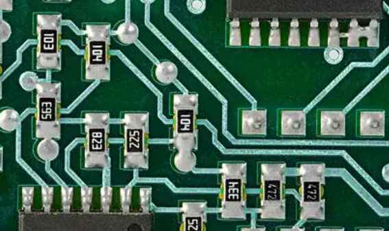
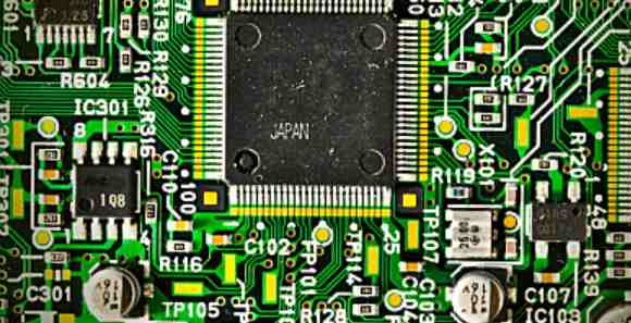
In a PCB board commonly used in switching power supply, usually each switching power supply has four current circuits, they are respectively input signal source current circuit, power switch AC circuit, output rectifier AC circuit, output load current circuit. The input loop charges the input capacitor through an approximate DC current, and the filter capacitor mainly plays a role of broadband energy storage. Similarly, output filter capacitors are used to store high-frequency energy from the output rectifier while eliminating DC energy from the output load loop. Therefore, the terminals of the input and output filter capacitors are very important, and the input and output current loops should be respectively connected to the power supply only from the terminals of the filter capacitors.
The setting and connection of input and output circuits are very important for the whole printed FPC circuit board, and whether it is reasonable or not will directly affect the size of electromagnetic interference. If the connection between the input and output loops and the power switch and rectifier loops cannot be directly connected to the terminal of the capacitor, the AC energy will be filtered by the input or output capacitor and radiated into the environment. The AC circuit of power switch and rectifier contains high amplitude trapezoidal current, which has a high harmonic component. Its frequency is much higher than the fundamental frequency of the switch. The peak amplitude can be up to 5 times of the continuous input and output DC current amplitude, and the transition time is usually about 50ns. These two circuits are the most likely to generate electromagnetic interference, so they must be laid before other printed wires in the power supply are routed.
In the input and input circuits of the LED switching power supply, each circuit is composed of three main components, which are filter capacitor, power switch or rectifier, inductor or transformer. These three important components should be placed next to each other and adjusted so that the current path between them is as short as possible. The best way to establish a switching power supply layout is similar to its electrical design. The best design process is as follows:
Place the transformer → Design the power switch current loop → design the output rectifier current loop → control circuit connected to the AC power circuit → design the input current source loop and input filter.


Just upload Gerber files, BOM files and design files, and the KINGFORD team will provide a complete quotation within 24h.