
Professional PCB manufacturing and assembly
Building 6, Zone 3, Yuekang Road,Bao'an District, Shenzhen, China
+86-13410863085Mon.-Sat.08:00-20:00

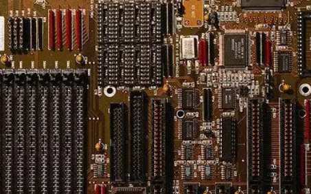
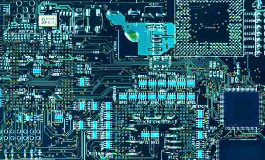
Hot air smoothing is to dip the printed circuit board into the molten solder (63SN/37PB), and then use the hot air to blow off the excess solder on the surface of the printed circuit board and in the metallized hole, to obtain a smooth, uniform and bright solder coating. After hot air leveling, the lead tin alloy coating layer on the printed circuit board surface should be bright, uniform and complete, with good weldability, no nodding and no semi-wetting, and coated with no exposed copper. Copper exposure on the surface of the pad and in the metallized hole after hot air leveling is an important defect in the inspection of finished products. It is one of the common reasons for hot air leveling and rework. There are many reasons for this problem, including the following ones.
1. The surface of the pad is unclean, and residual solder resistance contaminates the pad.
At present, most manufacturers use full-plate screen printing liquid photosensitive solder resistance ink, and then through exposure, development to remove excess solder resistance, get the time solder resistance pattern. In this process, the pre-drying process is not well controlled, the temperature is too high for a long time will cause difficulties in developing. Whether there are defects on the solder resistance negative, whether the composition and temperature of the developer are correct, whether the developing speed is correct, whether the developing point is correct, whether the nozzle is blocked and whether the pressure of the nozzle is normal, whether the washing is good, any of them will leave residual points on the pad.
For example, the copper exposure formed due to the negative is generally more regular, all at the same point. In this case, a magnifying glass can be used to find residual traces of solder resistance substances in the copper exposed area. Generally, a post should be set up to inspect the graphics and the inside of the metallized holes before the curing process, to ensure that the welding pad and metallized holes of the printed circuit board sent to the next process are clean and free weld ink residues.

2. Insufficient pretreatment and poor coarsening.
The quality of hot air leveling is greatly affected by the pretreatment process of hot air leveling. This process must completely remove the oil, impurities and oxide layer on the welding pad to provide fresh weldable copper surface for dipping tin. Now the more commonly used pre-treatment process is mechanical spray, the first is sulfuric acid - hydrogen peroxide micro-etching, micro-etching after acid immersion, and then water spray rinse, hot air dry, spray flux, immediately hot air leveling. Copper exposure caused by poor pre-treatment phenomenon is regardless of type of batch at the same time a large number of copper exposure points are often distributed throughout the board, especially on the edge.
Using a magnifying glass to observe the pre-treated circuit board will find obvious residual oxidation spots and stains on the pad. If similar situations occur, chemical analysis should be carried out on the micro-corrosion solution, check the second pickling solution, adjust the concentration of the solution to replace the solution that is seriously polluted due to too long use, and check whether the spray system is smooth. Appropriate extension of the treatment time can also improve the treatment effect, but it is necessary to pay attention to the phenomenon of over-corrosion. After the reworked circuit board is smooched by hot air, the post-treatment line is treated in 5% hydrochloric acid solution to remove the surface oxides.
3. Insufficient flux activity
The role of the flux is to improve the wettability of the copper surface, protect the laminate surface from overheating, and provide protection for the solder coating. If the activity of the flux is not enough, the wettability of the copper surface is not good, the solder can not completely cover the pad. The copper exposure phenomenon is similar to the poor pretreatment, and the extension of the pretreatment time can reduce the copper exposure phenomenon. Now the flux is almost all acid flux, containing acidic additives, such as too high acidity will produce serious copper biting phenomenon, resulting in high copper content in the solder cause lead tin rough; If the acid is too low, the activity is weak and will lead to copper exposure. If the copper content in the lead tin tank is large, copper should be removed in time. Process technicians choose a stable and reliable quality flux on hot air leveling has an important impact, excellent flux is the guarantee of hot air leveling quality.
In addition, other parameters also have an impact on hot air leveling, flux coating uneven, solder liquid level is too low, immersion time is wrong, wind and wind pressure adjustment is not good, wind knife position distance and so on May cause hot air leveling copper exposure problem. This problem is more intuitive, clear and easy to find and solve. The first inspection and inspection of products at any time when workers operate, timely feedback of problems, timely analysis and timely solution of technical personnel can greatly reduce the rework rate, provide product quality, and reduce the road copper phenomenon to a minimum.
PCB engineering design requirements
Apr 19,2023


Just upload Gerber files, BOM files and design files, and the KINGFORD team will provide a complete quotation within 24h.