
Professional PCB manufacturing and assembly
Building 6, Zone 3, Yuekang Road,Bao'an District, Shenzhen, China
+86-13410863085Mon.-Sat.08:00-20:00

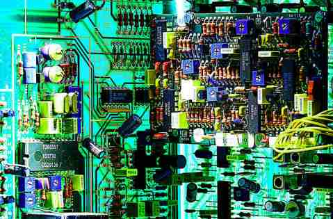
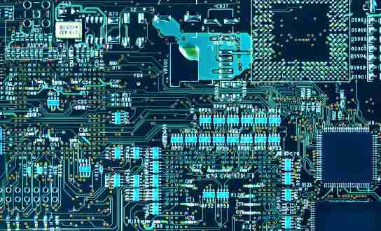
PCB, known as the "mother of electronic products", is mainly used in computer, communication, consumer electronics and other fields. The arrival of 5G era will enable China's PCB industry to grow more rapidly.
5G improves industry prosperity
According to the comparison between 4G and 5G, from the perspective of the number of base stations, 5G base stations may be 1.1 to 1.5 times of the current 4G base stations, and the number of micro-station construction may exceed 9 million stations. At the same time, it is estimated that the PCB value of 5G base station is about 12,500 yuan, which is about 3 times that of 4G base station in the past.
The combination of high price and large quantity of 5G PCB is bound to bring new driving force to the market of 5G PCB. It is estimated that China's 5G construction may reach its peak in 2022 to 2023, and the required PCB value will reach 12 billion yuan and 12.6 billion yuan respectively.
Electron permeability is expected to increase
Under the 5G trend, mobile phones still stuck in the 4G era will face big changes in their internal structure. 5G will likely consume more power than 4G phones, and the phones' internal batteries will likely continue to get bigger. The shortage of internal space is bound to drive the use of FPC in mobile phones to further increase; At the same time, SLP, as the PCB(excluding IC carrier board) with the minimum line width and line distance, further improves the internal integration of the mobile phone to help reduce the occupied space. In the 5G environment, the permeability is bound to continue to increase.
At the same time, 5G construction is accelerating, and the corresponding development of the Internet of vehicles is also expected to accelerate. Both intelligent network connection and automatic driving put forward extremely high requirements of strong real-time, low delay and high safety for the communication level of Internet of vehicles. In addition, the popularization of new energy vehicles and the gradual maturity of intelligent networked vehicles will greatly enhance the degree of automobile electronization (ADAS, cameras and millimeter-wave radar, etc.) in the future. It is expected that the growth of PCB products for automobile will be promising under the upgrading trend of automobile consumption.
The machine has the characteristics of high precision and high flexibility, the module structure design system can be customized according to the special production requirements of customers, and can be upgraded to meet the needs of future production development. The motion radius of the manipulator can cover the flux nozzle, preheating and solder nozzle, so the same equipment can complete different welding processes. The machine's unique synchronous process can greatly shorten the single board process cycle. The manipulator has the ability to make this selective welding with high precision and high quality welding characteristics. First of all, the precision positioning ability of the manipulator is highly stable (±0.05mm), to ensure that the production parameters of each plate are highly repeated and consistent; Secondly, the 5-D movement of the manipulator enables the PCB to contact the tin surface with any optimized Angle and orientation, so as to obtain the best welding quality. The tin wave height measuring needle installed on the manipulator splint device is made of titanium alloy. The tin wave height can be measured regularly under program control. The tin wave height can be controlled by adjusting the tin pump speed to ensure the stability of the process.

In spite of all the advantages mentioned above, the single nozzle solder wave drag welding process also has its shortcomings: the welding time is the longest in the three processes of flux spraying, preheating and welding. And because the solder joints are drag-welded one by one, the welding time will increase greatly with the increase of the number of solder joints, and the welding efficiency can not be compared with the traditional wave soldering process. The situation is changing, however, and multiple nozzle designs can maximize production. For example, double nozzles can be used to double production, and double nozzles can also be used for flux.
The immersion selective welding system has a number of solder nozzle, and the PCB solder joint is designed one to one, although the flexibility is not as good as the manipulator, but the output is equivalent to the traditional wave soldering equipment, the cost of the equipment is relatively lower than the manipulator. Depending on the size of the PCB, a single board or multiple boards can be transferred in parallel, and all spots to be soldered will be sprayed, preheated and welded in parallel at the same time. However, because of the different distribution of solder joints on different PCB, it is necessary to make special solder nozzle for different PCB. The size of the welding nozzle should be as large as possible to ensure the stability of the welding process and not affect the adjacent components on the PCB, which is important to the design engineer, but also difficult, because the stability of the process may depend on it.
The immersion selective welding process can be used to weld 0.7mm ~ 10mm solder joints. The welding process of short pins and small size pads is more stable and the possibility of bridging is small. The distance between adjacent solder joints, devices and welding nozzle should be greater than 5mm.


Just upload Gerber files, BOM files and design files, and the KINGFORD team will provide a complete quotation within 24h.