
Professional PCB manufacturing and assembly
Building 6, Zone 3, Yuekang Road,Bao'an District, Shenzhen, China
+86-13410863085Mon.-Sat.08:00-20:00


Board bubbling is one of the most common quality defects in the production process of circuit board. Because of the complexity of the production process of circuit board and the complexity of process maintenance, especially in chemical wet treatment, it is difficult to prevent the bubbling defects of board surface. Based on many years of actual production experience and service experience, the author now makes a brief analysis of the causes of bubbling on the copper plating surface of the circuit board.
The bubbling of the circuit board is actually the problem of poor binding force on the board, and then by extension, the surface quality of the board, which contains two aspects:
1. The cleanliness of the board;
2. Surface micro-roughness (or surface energy) problem; The bubbling problem on all circuit boards can be summarized as the above reason. The adhesion between the coatings is poor or too low, and it is difficult to resist the coating stress, mechanical stress and thermal stress generated in the production and processing process and assembly process in the subsequent production and processing process, resulting in different degrees of separation between the coatings.

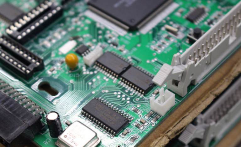
Keyou Circuit specializes in the production of PCB rapid proofing and batch, with high precision single side/double side/multilayer circuit board (1-26 layers), thermoelectric separation copper substrate, multilayer industrial control circuit board, medical circuit board, security PCB board, communication PCB board, automotive circuit board, composite bus copper substrate, foldable metal substrate, etc.
Some factors that may cause poor quality of the board in the process of production and processing are summarized as follows:
1. Problems of substrate processing; Especially for some thin substrate,(generally 0.8mm below), because the rigidity of the substrate is poor, should not be used to brush the plate, this may not be able to effectively remove the substrate production and processing process to prevent copper foil oxidation and special treatment of the protective layer, although the layer is thin, brush plate is easier to remove, but there are greater difficulties in chemical treatment, Therefore, in the production and processing of important attention to control, so as not to cause the poor bonding force between the substrate copper foil and chemical copper caused by the bubbling problem; This problem in the thin inner layer of blackening, there will also be bad blackening brown, uneven color, local black brown is not superior problems.
2. The surface of the board in machining (drilling, laminating, milling, etc.) process caused by oil or other liquids contaminated with dust pollution surface treatment phenomenon,
3. Copper sinking brush plate is bad: copper sinking before grinding plate pressure is too large, resulting in orifice deformation brush out orifice copper foil fillet and even orifice leakage substrate, so that in the process of copper plating, tin spraying and welding will cause orifice foaming phenomenon; Even if the brush plate does not cause leakage of the substrate, but the heavy brush plate will increase the roughness of the copper orifice, so in the process of micro-etching coarsening, the copper foil is easy to produce excessive coarsening phenomenon, there will be a certain quality hazard; Therefore, attention should be paid to strengthen the control of the brush process, the brush process parameters can be adjusted to the best through the wear mark test and water film test.
In the actual production process, there are many reasons for bubbling board surface, the author can only do a brief analysis, for different circuit board plant equipment technical level may appear different reasons caused by the bubbling phenomenon, the specific situation to be specific analysis, not generalize, copy; The analysis of the above reasons is not primary, secondary and important, basically according to the production process to do a brief analysis, in this series, just to provide you with a direction to solve the problem and a broader vision, I hope to everyone's process production and problem solving, can play a role in attracting jade!
What are the three major factors that cause PCB board welding defects?
PCB welding technology in recent years, the development of electronic industry process, we can notice a very obvious trend is reflow welding technology. The quality of PCB circuit board welding is also a problem that major electronic manufacturers pay close attention to. Please take a look at the three factors that cause PCB board welding defects together with the circuit board manufacturers.
1. Weldability of PCB board holes affects welding quality
Poor weldability of PCB board holes will produce virtual welding defects, affect the parameters of components in the circuit, lead to the instability of multilayer board components and inner wire conduction, and cause the functional failure of the entire circuit. The so-called welderability is the property of the metal surface being wetted by molten solder, that is, the metal surface where the solder forms a layer of relatively uniform continuous smooth adhesion film.
2. Welding defects caused by PCB board warping
PCB board and components in the welding process of warping, due to stress deformation and produce defects such as welding, short circuit. Warping is often caused by an imbalance in temperature between the upper and lower parts of the PCB board. For large PCB board, due to its own weight falling will also produce warping. A common PBGA device is about 0.5mm away from the PCB board. If the PCB board is large, the solder joint will be under stress for a long time as the PCB board returns to normal shape after cooling. If the device is raised by 0.1mm, it will be enough to cause a virtual welding open circuit.
3.PCB board design affects welding quality
In the layout, PCB board size is too large, although welding is easier to control, but the printing line is long, impedance increases, anti-noise ability decreases, cost increases; If it is too small, heat dissipation will decrease, welding is not easy to control, and adjacent lines will interfere with each other, such as electromagnetic interference of PCB board. Therefore, PCB board design must be optimized.
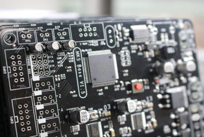
Keyou Circuit is a professional rapid production of high precision double-sided/multi-layer circuit board (1-26 layers),LED aluminum substrate, thermoelectric separation single-side/double-sided copper substrate, foldable metal substrate, special circuit board, industrial circuit board, power pcb board, medical circuit board, security PCB board, communication PCB board, automotive circuit board, instrument circuit board, military circuit board, etc.


Just upload Gerber files, BOM files and design files, and the KINGFORD team will provide a complete quotation within 24h.