
Professional PCB manufacturing and assembly
Building 6, Zone 3, Yuekang Road,Bao'an District, Shenzhen, China
+86-13410863085Mon.-Sat.08:00-20:00

In PCBA processing, there are mainly three kinds of commonly used electronic components repair: Chip component repair, multi-pin device repair and BGA repair.
(1) Repair of Chip components
Chip resistance, capacitance and inductance are usually called Chip components. The repair of Chip components is relatively simple. It can be repaired by ordinary soldering iron or simple repair equipment, but CHIP components are small. Otherwise too high temperature will cause the element to be damaged by heat.
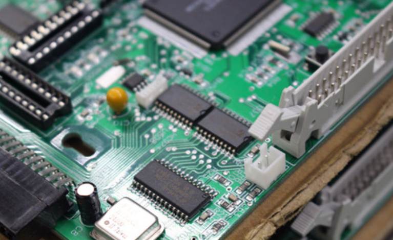
(2) Repair of multi-pin devices
For the repair of PLCC, LCCC, QFP and other multi-pin devices, the maintainer should have excellent welding skills, remove the devices on the circuit board to ensure the integrity of the circuit board, especially the welding pad is easy to be destroyed due to overheating or solder is not all melted. There are also some tips on how to dissolder better. For example, if you think the device is damaged, you can cut all the pins first, and then remove the individual pins much easier; For pins connected with a large area of coppered surface, it is necessary to use a high-power soldering iron to melt the solder, so as to complete the task before the heat is not transmitted out and has no effect on the surrounding devices.
When removing the welding device, the cooperation between the tin absorber and the soldering iron is very important, the timing should be until the molten state of the solder will be sucked out, the iron should be pushed to the center of the weld hole at the same time, so that the solder is sucked clean, must remember, with the heat of the iron rather than the force of the hand, if there is residual solder, it can be sucked out with a fine copper mesh, Solder - coated copper mesh is very good at tin absorption. Welding to avoid welding and short circuit, the correct welding principle is to fill the hole with as little solder as possible, and form a smooth cone at the pin.
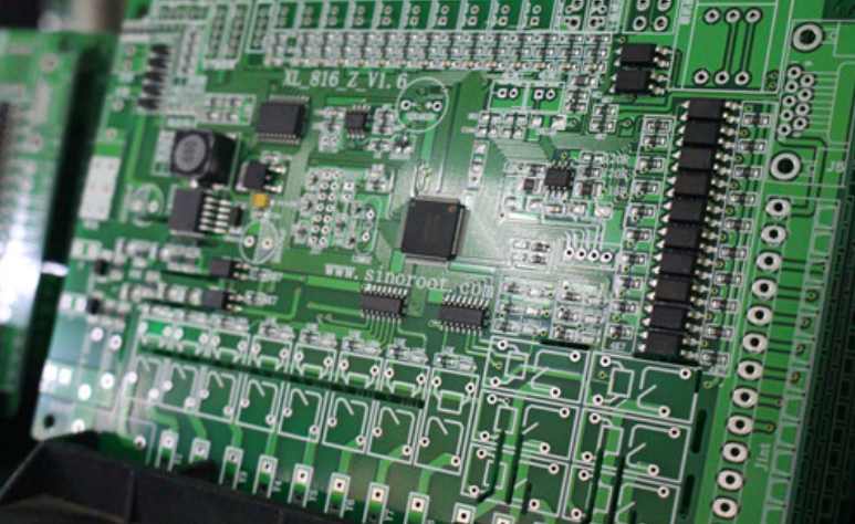
(3) Repair of BGA
The BGA repair platform is divided into optical alignment and non-optical alignment. The optical alignment is imaging through the optical module using a split prism. Non-optical alignment is to align the BGA according to the silk screen lines and points of the PCB board by the naked eye to achieve alignment repair. The repair process of BGA mainly includes dismantling BGA, cleaning pad, dewetting treatment, printing solder paste, mounting BGA and welding inspection.
To disassemble the BGA, the hot-air nozzle is connected to the device and heated to a certain temperature. Then, the suction nozzle suitable for disassembling the device is selected, the vacuum pressure of the suction device and the height of the suction nozzle are adjusted, and the BGA chip is removed. Pay attention to the uniform distance around the device. After the repair is completed, the welding will reset it; Cleaning pad is to clean and smooth the residual solder of PCB pad with soldering iron. It can be cleaned by dismantling braided tape and flat shovel iron head. Pay attention not to damage the pad and welding resistance film during operation; Moisture removal treatment refers to check the humidity display card of the opening device before installation, when indicating humidity > 20%, indicating that the device has been damp, the device should be placed in high temperature resistant anti-static plastic tray for baking; Printing solder paste must be used and BGA chip corresponding to the small template, template thickness and opening size should be determined according to the ball diameter and ball distance, generally we use ball planting process; BGA installation is to select an appropriate suction nozzle, open the vacuum pump, suck up the BGA device, shine the BGA pad printed with welding paste on PCB with the light source at the top of the camera, adjust the focal length to make the monitor display the clearest image, then pull out the BGA-specific reflective light source, shine the bottom of the BGA device and make the image the clearest, and then adjust the knob of the workbench. After making the bottom image of BGA device completely coincide with the image of PCB pad, the suction nozzle is moved down to mount the BGA device on the PCB circuit board, and then close the vacuum pump; Soldering and inspecting are similar to repairing other SMD devices.


Just upload Gerber files, BOM files and design files, and the KINGFORD team will provide a complete quotation within 24h.