
Professional PCB manufacturing and assembly
Building 6, Zone 3, Yuekang Road,Bao'an District, Shenzhen, China
+86-13410863085Mon.-Sat.08:00-20:00

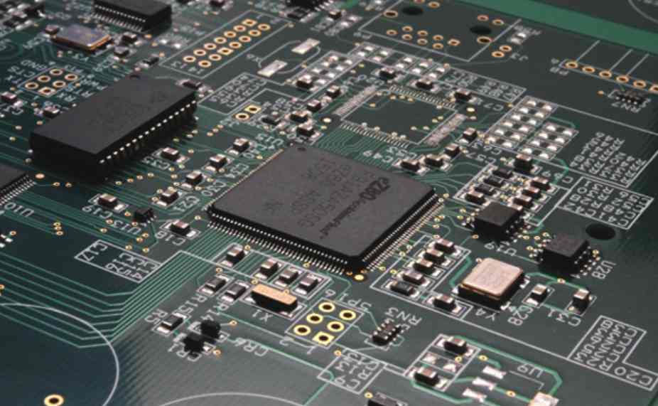
During the industry boom, many PCBA processing manufacturers will carry out PCBA outsourcing processing under the condition that they cannot normally schedule production. PCBA outsourcing processing means that PCBA processing manufacturers send PCBA orders to other powerful PCBA processing manufacturers. So, what are the general requirements of PCBA outsourcing processing?
One. Bill of Materials
Components shall be inserted or mounted in strict accordance with BOM, PCB silkscreen printing and outsourcing processing requirements. In case of material inconsistency with BOM, PCB silkscreen printing, or contradiction with process requirements, or ambiguous requirements, the operation cannot be carried out, contact the partner company in time to confirm the correctness of material and process requirements.
Two, anti-static requirements
1. All components are treated as electrostatic sensitive devices.
2. All personnel who come into contact with components and products should wear anti-static clothes, anti-static bracelets and anti-static shoes.
3. Anti-static packaging is adopted for electrostatic sensitive devices during raw materials entering the factory and warehousing.
4. In the process of operation, anti-static workbench is used, and components and semi-finished products are stored in anti-static containers.
5, welding equipment is reliably grounded, electric soldering iron is anti-static type. All need to be tested before use.
6. The semi-finished products of PCB board are stored and transported in anti-static boxes, and the isolation materials are anti-static pearl-cotton.
7. Use an ESD bag for a no-shell machine.
Iii. Provisions on the orientation of assembly of the appearance marks of components
1. Polar components are inserted according to polarity.
2. When the components (such as high-voltage ceramic capacitor) on the side of the screen are vertically inserted, the screen is facing right; When inserting horizontally, screen printing faces down. When the component (excluding the patch resistance) on the top of the screen is inserted horizontally, the direction of the font is the same as that of the PCB circuit board screen printing; In vertical interpolation, the top of the font faces right.
3. When the resistance is horizontally inserted, the error color ring faces right; When horizontal vertical insertion is made, the error color ring faces down. When the resistance is inserted vertically, the error color ring faces the plate.
Four, welding requirements
1. Pin height of insertion component on welding surface is 1.5 ~ 2.0mm. The patch element shall be flat on the surface, the solder joint shall be smooth and burr free, slightly arc shaped, and the solder shall exceed 2/3 of the height of the welding end, but shall not exceed the height of the welding end. Less tin, solder joint spherical or solder covered patch are bad;
2, solder joint height: solder climbing pin height single panel is not less than 1mm, double panel is not less than 0.5mm and need to be through tin.
3. Solder joint shape: conical and covered with the whole pad.
4, solder joint surface: smooth, bright, no black spots, flux and other sundries, no spikes, pits, pores, copper and other defects.
5, solder joint strength: fully wet with the pad and pin, no virtual welding, false welding.
6, solder joint section: component cutting foot as far as possible not cut to the solder part, in the pin and solder contact surface without cracking tin phenomenon. There are no spikes and barbs in the section.
7. Pin seat welding: pin seat requires the bottom plate insertion, and the position is correct, the direction is correct, after welding, the bottom floating height is not
More than 0.5mm, the seat body skew does not exceed the screen frame. Rows of needle pedestals should also be kept neat, not allowing dislocation or uneven
Five. Transportation
In order to prevent damage to the circuit board, the following packaging should be used during transportation:
1. Storage container: anti-static turnover box.
2, isolation material: anti-static pearl cotton.
3, placing distance: PCB board between the board, PCB board and the box have more than 10mm distance.
4, placing height: there is more than 50mm space from the top of the turnover box, to ensure that the turnover box stacked do not press to the power supply, especially the power supply with wire.
Six, washing requirements
Board surface should be clean, Wuxi beads, component pins, stains. In particular, the welding spot of the plug-in surface should not see any dirt left by welding. When cleaning the board, the following devices should be protected: wire, connecting terminals, relays, switches, polyester capacitors and other corrosive devices, and the relay is strictly prohibited to use ultrasonic cleaning.
Vii. All components shall not exceed the edge of the printed circuit board after installation.
8. When PCBA is over the furnace, due to the scouring of the pin of the plug-in element by tin flow, some plug-in elements will be tilted after welding in the furnace, resulting in the element body beyond the screen frame, so the welding personnel after the tin furnace is required to correct it properly.


Just upload Gerber files, BOM files and design files, and the KINGFORD team will provide a complete quotation within 24h.