
Professional PCB manufacturing and assembly
Building 6, Zone 3, Yuekang Road,Bao'an District, Shenzhen, China
+86-13410863085Mon.-Sat.08:00-20:00


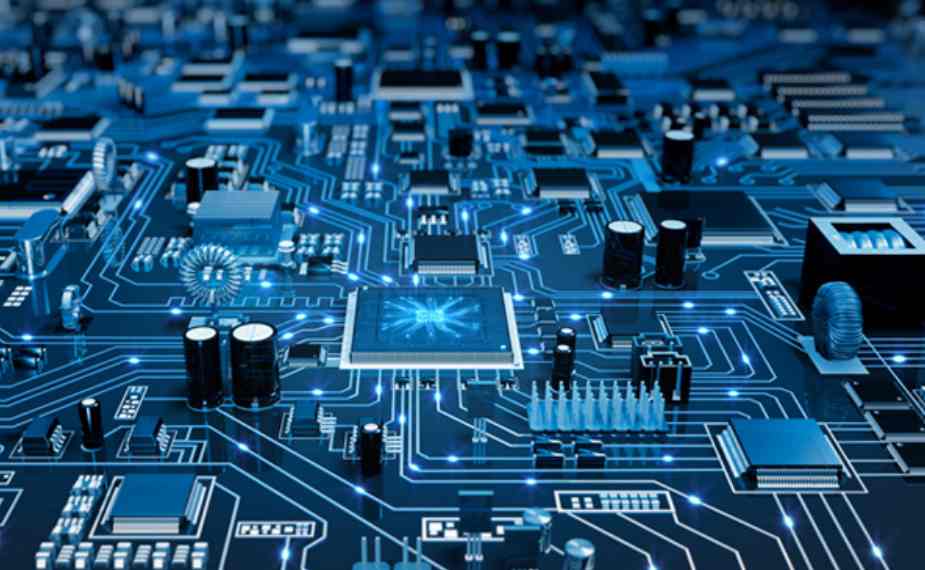
SMT(Surface-mount technology) is a technology for the production of electronic circuits in which components are mounted or directly placed on the Surface of printed circuit boards. In the industry, there are two methods: SMD (surface-mount device) and THT (through-hole technology). Both technologies can be used on the same printed circuit board, with the exception that punch and insert technology is applied to components that are not suitable for surface mount (such as large transformers, connectors, electrolytic capacitors, etc.). SMT components are usually smaller than punch inserts because they have smaller or no pins. They may be short pins or leads of various types and contact modes, or spherical matrix arrangements (BGA), etc.
SMT history
Surface mounting technology originated in the 1960s, and was initially developed by IBM, and gradually matured in the late 1980s. Originally designed by IBM in 1960 for use in a small computer, the computer was later used as an instrument component for the Saturn IB and Saturn V launch vehicles. The components are mechanically redesigned with minimal metal paging or end caps so that they can be soldered directly to the PCB surface. Components became smaller and were mounted surface-mounted on both sides of the PCB board, replacing punch and insert and allowing for higher line density. Usually only the welded joints hold the components to the plate. In rare cases, if some components are large or heavy, some adhesive may be used on the other side to prevent the components from falling off during reflow soldering. The adhesive is sometimes used to hold the SMT components on the other side of the SMT if SMT and punch inserts are processed simultaneously. In an alternative way, SMT and perforated components can be welded together without the aid of a binder if the SMT component is reflow soldering for the first time, thus the selective solder coating will be used to prevent the component from soldering during reflow soldering and the component from floating during wave soldering. The surface mount itself leads to a degree of automation, reducing labor costs and significantly increasing production efficiency. SMD components are one-quarter to one-tenth the size and weight of a punched cartridge component, and cost one-half to one-quarter.
SMT terminology
Because surface mount is a production technology, there are many different terms, especially when in different production environments, there are components, technologies, and equipment that need to be distinguished significantly. Mainly contains terms in the following table:
Terminology interpretation
SMD: Surface mounted components (active, passive and electromechanical components)
SMT: Surface mount technology (assembly and welding technology)
SMA: Surface assembly process (modular assembly using SMT)
SMC: Surface-mounted components (i.e. components for SMT)
SMP: Surface mount package (SMD component package)
SME: Surface mount equipment (SMT assembly equipment, etc.)
SMT surface mount technology
The position of the surface mounted components needs to be smooth, usually solder, silver or gold and no through hole welding position is called "pad". Solder paste, a viscous substance consisting of a lead-tin component and a solder aid mixture, penetrates through a stainless steel or nickel steel mesh to attach to the pad with the help of a solder paste press, which can also be done by printing, similar to an inkjet printer. After the solder paste is printed, the circuit board will be pasted through the corresponding conveyor belt after picking up and placing equipment. The components to be affixed are usually placed in paper or plastic pipes and mounted on SMT machines with Feida. Some of the larger integrated circuits will be delivered via anti-static trays. SMT equipment takes out corresponding components from Feida and pastes them onto PCB. Because the solder paste on PCB has certain viscosity, the components on the pad have good adhesion effect.
At this point, the PCB board will be transferred to the reflow soldering furnace. There is a preheating zone at the head of reflow welding, where the temperature of the circuit board and components gradually rises and then enters the high temperature zone. The solder paste will melt and bind the pad and components. The surface tension of the melted solder paste will allow the components to remain in the position without deviation, and even the surface tension will automatically pull the slightly offset components back to the correct position. There are a variety of reflow welding techniques. One uses red lights (known as infrared reflow soldering), another uses hot gas convection, and one of the most popular techniques uses special high-boiling fluorocarbon liquids (known as steam reflow soldering). The technology was gradually abandoned after lead-free regulations were introduced due to environmental concerns. Prior to 2008, standard air or nitrogen convection reflow was the norm. Each approach has its advantages and disadvantages. With infrared irradiation, PCB designers must be aware that short components are not obscured by tall components, but component location is not a consideration if the designer is aware that steam reflow or convection reflow welding is used during manufacturing. During reflow soldering, some non-conventional or heat-sensitive components need to be welded by hand, but for a large number of such components, the corresponding reflow welding process needs to be completed by infrared beams or convection equipment.
If the PCB is a double-sided design, all solder paste printing, mounting and reflow soldering processes need to be repeated to attach the component to the specified position by solder paste or red glue. If the model wave soldering process is required, the components need to be adhered to by red glue to prevent the components from falling off due to the melting of solder in the process of wave soldering.
After the welding process is complete, the panel is cleaned to remove the rosin flux and some of the tin balls to prevent them from short-circuiting between the components. Rosin fluxes are removed by fluorocarbon solvents, high-ignition hydrocarbon solvents, or low-ignition solvents such as lemon extract from orange peel. The water-soluble flux is removed with ionized water and a cleaner, then the surface moisture is quickly removed using an air knife. However, most indiscriminate mounting is performed without a cleaning process, that is, the rosin flux will remain on the surface of the PCB board, which will save cleaning costs, improve production efficiency, and reduce waste.
Some SMT SMT Connecting Electronics manufacturing standards, such as IPC (Association Connecting Electronics Industries) need to implement cleaning standards to ensure the PCB board is clean, and even some fluxes that do not need cleaning must be removed. Proper clarity will clean up the unrecognizable flux, dirt and impurities between the lines. However, not all manufacturers strictly follow IPC standards and display them on the board, or customers simply don't care. In fact, many manufacturers' production standards are more stringent than IPC standards.
Finally, the PCB board needs to be inspected to see whether the components are missing, wrong direction, welding, short circuit, etc. If necessary, the defective board should be sent to a professional repair table for repair, such as ICT testing or FCT functional testing, until the test PCB circuit board works properly.
Advantages and disadvantages of SMT
Feb 28,2023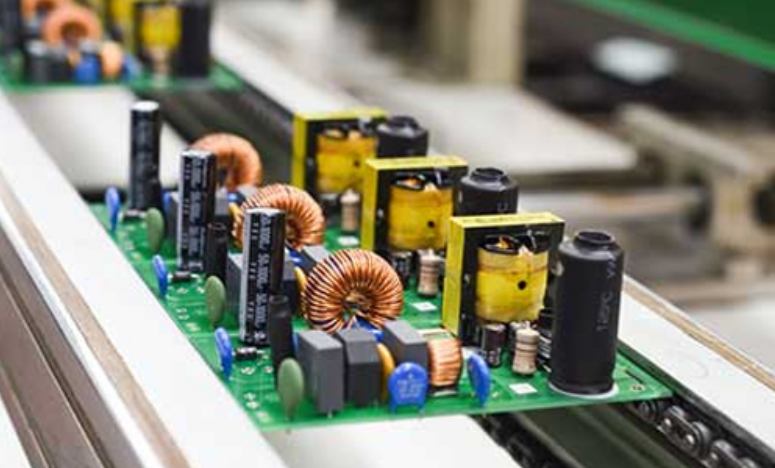


Just upload Gerber files, BOM files and design files, and the KINGFORD team will provide a complete quotation within 24h.