
Professional PCB manufacturing and assembly
Building 6, Zone 3, Yuekang Road,Bao'an District, Shenzhen, China
+86-13410863085Mon.-Sat.08:00-20:00

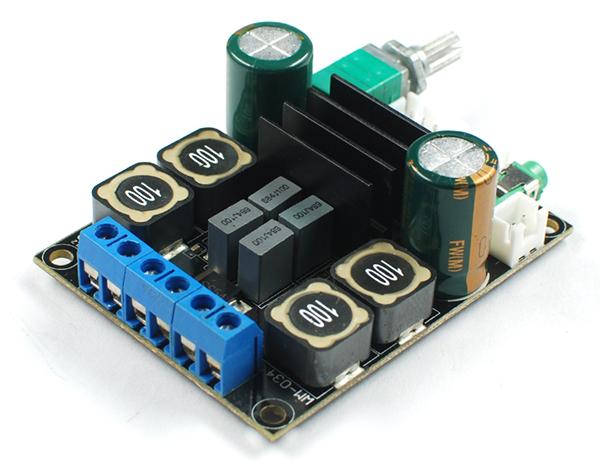
Factors affecting PCB welding quality
From PCB design to the completion of welding of all components into a high quality circuit board, PCB design engineers and even the level of welding process, welding workers and many other links have strict control.
There are mainly the following factors: PCB diagram, the quality of the circuit board, the quality of the device, the oxidation degree of the device pin, the quality of the solder paste, the printing quality of the solder paste, the accuracy of the program of the placement machine, the mounting quality of the reflow furnace temperature curve setting and so on.
Welding plant itself can not surmount the link is PCB drawing link. Because people who do circuit design often do not weld circuit boards so that they can not get direct welding experience, do not know the various factors affecting welding; And welding factory workers do not understand the drawing board, they just finish the production task, have no mind, more have no ability to analyze the causes of bad welding. Due to the two aspects of the talent in their respective roles, it is difficult to organically combine.
Suggestions for PCB drawing
About the positioning hole
Four holes (minimum aperture 2.5mm) should be left at the four corners of the PCB board for positioning the circuit board when printing solder paste. I want the center of the X or Y axis to be on the same axis.
About mark point
For placement machine positioning. The printed circuit board should be marked with the Mark point, the specific position: it can be a round or square pad on the diagonal of the board, and do not mix with the pad of other devices. If there are devices on both sides, both sides should be marked.
When designing PCBS, please note the following:
1. The shape of Mark point should be symmetrical up and down or left and right
2. The size of A is 2.0mm.
3, from the outer edge of the Mark point 2.0mm away from the range, there should be no shape and color changes that may cause wrong identification. (pad and paste)
4. The color of Mark point should be different from the color of PCB around it.
5, in order to ensure the accuracy of identification, the surface of the Mark point is plated with copper or tin to prevent surface reflection. The shape is only marked by lines, light points can not be recognized.
About leaving 5mm edge
When drawing PCB, no less than 3mm edge should be left in the long side direction for the placement machine to transport the circuit board, and the placement machine cannot mount devices within this range. Do not place patch devices within this range.
The circuit board with devices on both sides should be taken into account the second time over reflux will be welded side of the side of the device off, serious will rub off the pad, destroy the circuit board.
Therefore, it is recommended not to place the patch device within 5mm from the long side of the less side of the chip (generally the Bottom surface). If indeed due to the limited area of the circuit board, you can add the process edge in the long side.
Do not directly hole the pad
The defect of passing directly through the hole on the pad is that the solder paste melts into the hole during overreflux, resulting in the lack of tin on the device pad, thus forming virtual welding.
Polarity labeling of diode and tantalum capacitor
Polarity marking of diode and tantalum capacitor should conform to industry regulations, so as not to weld the wrong direction by experience.
About screen printing and signage
Please hide the device model. Especially the circuit board with high device density. Otherwise, dazzle the effect of finding the welding position. And don't just label the model, not the label. The size of a silk screen character should not be too small to read. Character placement should be staggered over holes to avoid misreading.
The IC pad should be extended
When drawing PCB for IC packaging such as SOP, PLCC and QFP, the pad should be extended. It is appropriate that the pad length on PCB =IC foot length ×1.5, so that when manual soldering iron is used, chip pins and PCB pad and tin are fused into one.
Width of IC pad
SOP, PLCC, QFP package IC, drawing PCB should pay attention to the width of the pad, pad a width on the PCB =IC foot width (i.e., Nom in datasheet. Value), please do not widen, ensure that b(i.e., between two pads) has enough width, so as not to cause continuous welding.
Do not close together two devices of higher thickness
The tight cloth will cause the SMT machine to touch the previous attached device when attaching the second device, and the machine will detect the danger, resulting in automatic power failure.
About BGA
Because the BGA package is special, its pad is under the chip, and the welding effect can not be seen outside. In order to facilitate the repair, it is recommended to make two positioning holes with Hole Size:30mil on the PCB board, so as to locate the steel mesh (used to scrape the solder paste) during the repair.
Warm tip: The size of the positioning hole should not be too large or too small. It is appropriate to make the needle not fall off after insertion, not shake, and a little tight when insertion, otherwise the positioning is inaccurate.
And it is suggested that the space should be set aside within a certain range around the BGA to place the device, so as to be able to put the screen scraping paste when repairing.
About PCB board color
Don't make it red. Because the red circuit board is white under the red light source of the camera of the patch machine, it cannot be programmed and is not convenient for the welding of the patch machine.
It's about the smaller devices underneath the larger devices
Some people like to arrange small devices under the same layer of large devices, so the layout will cause difficulties to repair, repair must be removed first, and may cause damage to the digital tube. It is recommended to drain the resistance under the digital tube to the Bottom surface.
About the effect of copper coating on solder joint
Because the copper coating will absorb a lot of heat, resulting in the solder is difficult to fully melt, resulting in the formation of virtual welding.
summarize
Nowadays, more and more engineers can draw, wire and design PCB with software. However, once the design is completed, the welding efficiency can be improved. The author believes that the above factors need to be paid attention to. And cultivate good drawing habits, good communication with the processing plant, is every engineer to consider.


Just upload Gerber files, BOM files and design files, and the KINGFORD team will provide a complete quotation within 24h.