
Professional PCB manufacturing and assembly
Building 6, Zone 3, Yuekang Road,Bao'an District, Shenzhen, China
+86-13410863085Mon.-Sat.08:00-20:00

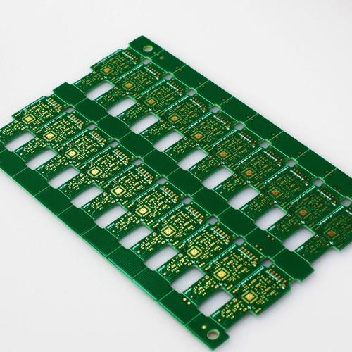
PCB circuit board appearance disposal process covers: oxygen resistant circuit board, spray tin circuit board, lead-free spray tin circuit board, sunk gold circuit board, sunk tin circuit board, sunk silver circuit board, plated gold circuit board, gold finger circuit board, nickel palladium gold OSP circuit board, etc. The main requirements are: low cost, good weldability, mean storage conditions, short time, environmental protection technology, good welding, smooth. Spray tin: Spray tin plate is generally multi-layer (4-46 layers) high precision PCB circuit board.
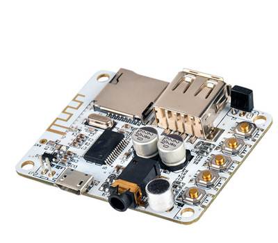
Gold fingers (connecting finger) are connecting devices between memory strips and memory slots. All signals are transmitted through gold fingers. Gold finger is composed of a lot of golden conductive contact pieces, because of its plated appearance and conductive contact pieces arranged like fingers, so it is called "gold finger", gold finger plate is gold-plated or gold-plated. The gold finger is actually coated with a layer of gold after a special process on the copper coated plate, because gold has strong oxygen resistance and high conductivity. However, due to the extremely expensive price of gold, until now, more memory is considered appropriate and use tin to replace it. Since the beginning of the 1990s, tin has been popularized. Until now, the "gold finger" of motherboard, memory and video card facilities is almost used as appropriate and tin material. Only local high performance server/office accessories contact points will then be considered appropriate and the use of gold plating, the price is not low.
Gold deposition is considered appropriate and the use of chemical deposition method, after chemical oxygen recovery reaction method to generate a layer of coating, ordinary thickness is thick, is a kind of chemical nickel gold deposition method, can reach a thicker gold layer.
Gold plating is considered appropriate and the use of the principle of electrolysis, also called electroplating form. Other metal surface disposal is also most considered appropriate and the use of electroplating form.
In the actual product application, 90 percent of the gold plate is sunk gold plate, due to the poor welding performance of the gilt plate is his fatal lack, but also the direct cause of many enterprises to compromise the gilt process!
Gold deposition process on the printed circuit board appearance of solid color, good cleanliness, smooth coating, satisfactory weldability of nickel gold coating. Basically, it can be divided into four stages: pre-treatment (oil removal, micro-etching, activation, post-leaching), nickel sedimentation, gold sedimentation, and post-treatment (waste gold water washing, DI washing, baking). The thickness of the gold deposit is between 0.025 and 0.1um.
Gold is used in the appearance of the circuit board, due to the strong electrical conductivity of gold, good oxygen resistance, long life, common applications such as button board, gold finger circuit board, and the basic difference between gold plate and gold plate is that gold is hard gold (wear-resistant), gold is soft gold (not wear-resistant).
1, sinking gold circuit board and gold-plated circuit board formed by the crystal structure is different, sinking gold for gold thickness is thicker than gold, gold will be golden, more yellow than gold (this is one of the ways to distinguish gold and sinking gold), gold will be slightly white (nickel color).
2, the crystal structure of the gold-plated circuit board and the gold-plated circuit board is different, the gold-plated phase is easier to burn welding, will not lead to bad welding. The stress of the gold plate is easier to control, and it is more helpful to the processing of the products. At the same time, because the gold is softer than the gold, so the gold plate is not wear-resistant to make gold fingers (the lack of gold plate).
3, sinking gold circuit board only on the pad nickel gold, skin effect signal transmission is in the copper layer will not have an impact on the signal.
4, gold board than gold plated crystal structure is more detailed and precise, not easy to produce oxygen.
5, with the PCB processing precision requirements more and more high, line width, spacing has reached below 0.1mm. Gilding is easy to generate gold wire short circuit. Sunk gold circuit board only on the plate nickel gold, so can not help but easily produce gold wire short circuit.
6, sinking gold circuit board only on the welding plate nickel gold, so the welding on the line and the copper layer of the joint is stronger. The project will have no effect on spacing initiation at the time of payment.
7, for the higher requirements of the wrench, the flatness requirements are better, generally it is considered appropriate and the use of gold, gold will not reveal the black pad phenomenon after assembly. The flatness and service life of the gold plate is better than that of the gold plate.
Flatness and life expectancy
Feb 13,2023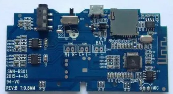


Just upload Gerber files, BOM files and design files, and the KINGFORD team will provide a complete quotation within 24h.