
Professional PCB manufacturing and assembly
Building 6, Zone 3, Yuekang Road,Bao'an District, Shenzhen, China
+86-13410863085Mon.-Sat.08:00-20:00

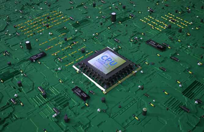
Printed circuit boards (PCBS) can be found in almost every application in any industry. Networking and communications applications are no exception. These boards help communicate, which is an easy task. In these applications, printed circuit boards can be manufactured from different materials. What are these materials? Would you like to know? The following article illustrates the different materials used to manufacture PCBS for networking and communication applications. Again, various useful features and characteristics of these materials are discussed in the post. Read on to learn more.
Networking and Communication What are the different materials used in PCBS?
The structure and design of a printed circuit board depends on its application. Similarly, for networking and communication applications, different materials can be used for PCBS. Here are some of the most commonly used materials:

370HR: 370HR is basically prepreg and laminate for printed circuit boards. Printed circuit boards made using 370HR meet RoHS requirements. The most common problem in PCBS is conductive anode wire (CAF), which is an electrochemical corrosion process. In this case, the copper metal at the anode dissolves and moves to the cathode. This can cause electrical short circuits, which are bad for any application, especially networking and communications. However, 370HR PCB is resistant to CAF. In addition, they have high density interconnections and excellent thermal reliability.
Glass epoxy FR4: Glass epoxy FR4 material has excellent strength-to-weight ratio. In addition, this material is a general purpose high pressure thermosetting laminate. This makes it suitable for networking and communication applications. Epoxy glass FR4 PCBS maintain electrical insulation and excellent mechanical properties under all conditions (dry or wet). In addition, the material has excellent mechanical strength and is known for its near-zero water absorption.
High speed Pyralux TK: High speed Pyralux TK materials are mainly used in PCB for high frequency applications. Traditional knowledge refers to Teflon-Capton. The copper-clad bond and laminate are usually double-sided. The bond layer used in the material helps protect it from harsh environments and provides good electrical insulation. Fluoropolymers and polyimides are used to make primary composites. TK materials are specifically designed for flexible digital circuit boards. Further advantages of this material include low moisture absorption, better flexibility and low dielectric constant.
Polyimide: This is another material that is most commonly used in networking and communication PCBS. The main advantage of this material is its excellent thermal stability. This allows the material to withstand extremely high heat in some applications. PCBS that are known to use polyimides provide a good basis for surface mounting. In addition, it is a cost-effective material choice for PCBS.
Now that you know what the different materials are for manufacturing PCBS for networking and communication applications, it will be easier for you to choose the right materials according to our requirements. Are you still confused about choosing the right materials? In this case, it is recommended to consult an expert who can guide you in choosing the right material for your PCB.
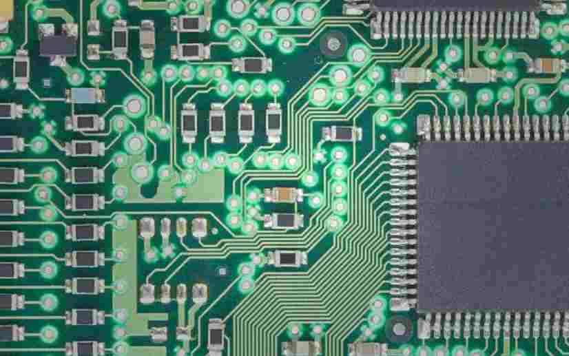
4 Tips for High speed high density PCB design
In the case of fixed board size, it is often necessary to increase the track density of the PCB if more functionality is required in the design, but this can lead to increased mutual interference of the tracks, which are also so thin that the impedance cannot be reduced. . Crosstalk interference should be considered when designing high speed, high density PCBS, as it can greatly affect timing and signal integrity. Here are some considerations:
1. Control the continuity and matching of trace characteristic impedance.
2. Trace space. The spacing is usually seen to be twice the width of the line. Simulation can be used to understand the effect of route spacing on timing and signal integrity, and to find out the minimum allowable space. The results can vary from chip to chip. Select the appropriate termination method. Avoid adjacent layers running in the same direction, or even overlapping each other, because the crosstalk is greater than the crosstalk of adjacent lines in the same layer.
3. Use blind/buried holes to increase track area. However, PCB board manufacturing costs will increase. It's really difficult to achieve full parallelism and the same length in a real implementation, but still try to do it.
4. Differential terminals and common-mode terminals can be retained to mitigate the impact on timing and signal integrity.


Just upload Gerber files, BOM files and design files, and the KINGFORD team will provide a complete quotation within 24h.