
Professional PCB manufacturing and assembly
Building 6, Zone 3, Yuekang Road,Bao'an District, Shenzhen, China
+86-13410863085Mon.-Sat.08:00-20:00


Prevent SMT OEM defects and X-ray inspection
Prevent OEM defects SMT casting production
Some common undesirable phenomena may occur in the OEM produced by smt. These problems affect the quality of products processed by SMT wafer processing plants. So, how to prevent these undesirable phenomena in electronic processing?
1. Poor wettability
Poor wetting means that during welding, the welding area of solder and substrate will not produce metal to metal reaction after wetting, resulting in missed welding or fewer welding failures.
Solution: select appropriate welding process, take anti fouling measures on the surface of base plate and components, select appropriate solder, and set reasonable welding temperature and time.
2、 Bridging
Most of the reasons for bridging in smt casting production are due to excessive solder or serious edge collapse after solder printing, or the size of the solder area of the substrate exceeds the tolerance, installation offset, etc., and the circuit tends to be miniaturized., Bridging will lead to power short circuit, affecting the use of products.
Circuit board

Solution:
1. The bad edges shall be prevented from collapsing during solder paste printing.
2. When designing the size of PCBA base plate welding area, pay attention to the design requirements of OEM processing.
3. The installation position of components shall be within the specified range.
4. The wiring clearance of PCBA base plate and the coating accuracy of solder resist must be strictly required.
5. Establish appropriate welding process parameters.
3. Crack
When the welded PCB just leaves the welding area, due to the difference in thermal expansion between solder and connecting parts, under the effect of rapid cooling or rapid heating, due to the influence of solidification stress or shrinkage stress, SMD will basically produce microcracks. In the process of stamping and transportation, the impact stress and bending stress on the SMD must also be reduced.
Solution: When designing surface mount products, we should consider narrowing the thermal expansion gap and correctly setting the heating and cooling conditions. Use solder with good ductility.
4、 Tin ball
In the welding process of Shenzhen smt casting production, due to rapid heating, when the solder is dispersed, welding balls will be produced in most cases. In addition, it is also associated with undesirable phenomena such as dislocations, sagging and solder contamination.
Solution:
1. Prevent welding and heating too fast and defects.
2. Prevent solder sagging, dislocation and other defective products.
3. The use of solder paste must meet the SMT processing requirements
4. The corresponding preheating process shall be implemented according to the welding type.
Principle and Application of X-ray Testing
With the continuous development of electronic technology, surface mount technology is becoming more and more popular, the size of single-chip chips is becoming smaller and smaller, and the pins of single-chip chips are gradually increasing, especially the BGA single-chip chips that appear in recent years. Since the pins of the BGA single chip microcomputer chip are not distributed around according to the traditional design, but on the bottom of the single chip microcomputer chip, it is undoubtedly impossible to judge the quality of the solder joints according to the traditional manual visual inspection. It must be based on ICT or even functional testing. However, under normal circumstances, if there are batch errors, they cannot be found and corrected in a timely manner. Manual visual inspection is the most inaccurate and reproducible technology. In addition, this X-ray inspection technology has been more and more widely used in the post weld inspection of SMT reflow welding. It can not only conduct qualitative and quantitative analysis of solder joints, but also find faults and correct them in a timely manner.
1. Working principle of X-ray machine:
When the circuit board enters the machine along the guide rail, there is an X-ray emission tube above the circuit board. The X-ray emitted by the circuit board passes through the circuit board and is received by the detector (usually the monitor) below. Lead absorbs X-ray. In comparison with X-ray passing through glass fiber copper, silicon and other materials, X-ray irradiated on solder joints is largely absorbed, and the appearance of black spots produces good images, which makes the analysis of solder joints very simple and intuitive. In addition, a simple image analysis algorithm can automatically and reliably detect solder joint defects.
2. X-ray technology:
X-ray technology has evolved from the previous two-dimensional detection method station to the current three-dimensional detection method. The former is a projection X-ray detection method, which can generate clear visual images of periodic solder joints on a single panel. However, for the widely used double-sided reflow soldering board, the effect of surface reflow soldering is very poor, which makes the visual images of solder joints on both sides overlap and is extremely difficult to distinguish. However, the latter 3D detection method uses layered technology to focus the beam on any layer and project the corresponding image onto the rotating receiving surface at a high speed. Because the receiving surface tells the rotation, the image at the intersection is very clear, while the image on other layers is eliminated. The 3D detection method can independently image the solder joints on both sides of the circuit board.
In addition to detecting double-sided welded plates, 3D X-ray technology can also conduct multi-layer image slice detection on invisible solder joints such as BGA, that is, thoroughly detect the top, middle and bottom of BGA solder joints. This method can also be used to measure through hole PTH solder joints to check whether there are enough solder joints in the through hole, thus greatly improving the connection quality of the solder joints.
3. X-ray instead of ICT
With the increasing density of PCB, SMT equipment becomes smaller and smaller, and the point space left for ICT test in PCB design becomes smaller and smaller, or even cancelled. In addition, for complex printing, if the circuit board is directly sent from the SMT production line to the function test location, it will not only lead to a decline in the pass rate, but also increase the cost of fault diagnosis and maintenance of the circuit board, even lead to a delay in delivery, and lose competitiveness in today's highly competitive market. If X-ray inspection is used instead of ICT at this time, it can ensure the production path of functional test and reduce fault diagnosis and maintenance work. In addition, using X-ray for spot inspection in SMT production can reduce or even eliminate batch error. It is worth noting that for solders that cannot be detected by ICT, there is too little or too much solder, and cold sweat, solder or porosity and other X-rays can also be measured. These defects can easily pass ICT or even functional tests without being found, thus affecting the product life. Of course, X-ray cannot detect the power defects of the equipment, but these defects can be detected in the functional test. In short, adding X-ray testing will not only miss any defects in the manufacturing process, but also detect some defects that ICT cannot find.
Based on the above factors, the 3DX ray machine can evaluate the size, shape and characteristics of each SMT solder joint, and automatically detect unacceptable and critical solder joints Key solder joints are those that will lead to premature product failure Of course, in other tests, these key solder joints will be considered as good solder joints

Second hand SMT wire placement machine
Dec 02,2022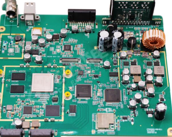


Just upload Gerber files, BOM files and design files, and the KINGFORD team will provide a complete quotation within 24h.