
Professional PCB manufacturing and assembly
Building 6, Zone 3, Yuekang Road,Bao'an District, Shenzhen, China
+86-13410863085Mon.-Sat.08:00-20:00


SMT reels and bulk and microstrip transmission lines
Pallet and bulk data SMT chip replacement processing
When purchasing components for SMT chip processing, data packaging is very important! Most component distributors provide the same components in multiple packages to accommodate different selection and placement loading preferences SMT patch data package mainly includes: bulk data, pallet data, pallet, tube and batch Each packaging type has its advantages, and it is difficult to determine which packaging type is most suitable for a particular job
Panel data and bulk data
The tape and reel of bulk materials are transported to the picking machine through the tape containing parts (usually small integrated circuit). However, the main difference is the length of the tape. The "cutting tape" provides parts in the form of small pieces of tape, while the "disc packaging material" is long and continuous and wrapped in the disc packaging material. Although its use depends on the type of board to be assembled, tray information is usually a better and more common option.
The biggest advantage of roll packaging is time. There is no need to load 20 separate tapes, and the reel can be continuously fed only once the operator loads it into the feeder.
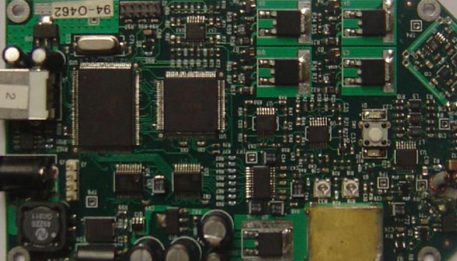
Circuit board

In addition, quality standards require operators to notify quality control (QC) person every time a new component is loaded into the machine According to the principle of economy, this is waste
SMT tray information also allows the operator to avoid paper jams. The cut tape will sometimes get stuck in the paper feeder, and various parts of the drum will often avoid paper jam. However, it is absolutely necessary to cut the tape when only a few specific types of components are required for the circuit board. It is important to keep this in mind during the procurement phase.
Other common packaging
Although cut tape and roll packaging are usually the most commonly used packaging, there are many other types of packaging available. Let's briefly describe the other two options to make the best packaging decision for your specific line.
Pallet information
Trays are typically used for larger surface mount racks such as QFN and BGA. Pallets require less wear because larger components are much more expensive. Although fewer parts are usually used when transporting parts, more protection is provided when using the pipe.
The purchase of smt patch data is very important. A qualified board is composed of qualified data. In addition, attention should be paid to the packaging method of data when purchasing data
Microstrip Transmission Line in RF PCB Design
So far, microstrip is still the most commonly used transmission line structure in RF and microwave design. However, with the increasing speed and density of digital and hybrid technology design, this situation is becoming less and less.
Because for the same impedance, the microstrip line is generally wider than the stripline, and because of the new radiation related to the microstrip line, it requires more wiring space and greater distance to record nearby traces. In a pure RF or microwave design, this is usually not a problem, but with the demand for smaller product sizes and the consequent increase in component density, it becomes difficult to obtain.
Structure
The microstrip transmission line consists of a conductor (usually copper) with a width of W and a thickness of t. The conductors are routed on a wider ground plane than the transmission line itself and are separated by a dielectric of thickness H. The best practice is to ensure that the ground reference plane extends at least 3H on both sides of the surface microstrip path.
Favorable conditions
·Historically, the main advantage of microstrip lines may be the ability to use only two layers of boards, with all components mounted on one side. This simplifies the manufacturing and assembly process and is the lowest cost RF circuit board solution. Since all connections and components are on the same surface, it is unnecessary to use through holes when connecting. In addition to the cost factor, this is also ideal, because the use of vias does not add capacitance or inductance.
·For the same impedance, the microstrip line is usually wider than the stripline. Since the etching tolerance in manufacturing is an absolute value, it is easier to control the characteristic impedance of the track more strictly. This is a very small percentage change if the track width is 20 mils and the width is reduced by 1 mil by over etching. For example, in FR408 data, a microstrip trace with a dielectric constant of 3.8, 20 mils higher than the ground, and 11.5 mils higher will produce about 50.8 ohms. If this trajectory is reduced to 19 mils, the characteristic impedance will be approximately 52.6 ohms and the characteristic impedance will increase by 3.6%. In the same data, a 5mil stripline with 6 mils of upper and lower grounding will produce about 50.35 ohms, but when 1 mil is reduced to 4 mils, the characteristic impedance will be about 56.1 ohms, an increase of 11.5%. When some designs are completed, the characteristic impedance of the final track is not specified, but the final width is specified. In the same over etching scheme, a reduction of 5 million traces of 1 million mils will reduce the final trace width by 20%, and a reduction of 20 mils of 1 million mils will reduce the width by 5%.
Disadvantages
·Since microstrip transmission lines are usually very wide and laid on the surface of the circuit board, this means that the surface area available for component placement will be reduced. This makes microstrip useless for high-density hybrid technology design, which almost always has space value.
·Microstrip transmission lines will radiate more than other transmission line types, which will be the main contributor to the overall radiation EMI of the product.
·Third, with the increase of microstrip radiation, crosstalk becomes a problem. It is necessary to increase the spacing with other circuit components, which will reduce the available wiring density.
·Microstrip designs often require an external mask, which adds cost and complexity. In fact, this has become one of the most important issues in the design of mobile phones and other portable devices. The driving force of many products is getting smaller and smaller. This means that the mask layer will be closer to the surface of the circuit board, which will increase the capacitance of each tissue length of the transmission line, thus changing its impedance. Consider carefully when choosing to use microstrip transmission lines and derive impedance models. If the track needs to pass through the outer mask wall, you may need to change the transmission line width a short distance, usually through a "tunnel", which is usually closer to the panel surface than the top of the mask.
·The characteristic impedance of the microstrip will be affected by solder resist or other surface coatings From one manufacturer to another SMT manufacturer, or even from one board of directors of the same supplier to another, the application of these coatings may be very inconsistent Therefore, the influence of these coatings on the impedance of surface microstrip line is not clear


Just upload Gerber files, BOM files and design files, and the KINGFORD team will provide a complete quotation within 24h.