
Professional PCB manufacturing and assembly
Building 6, Zone 3, Yuekang Road,Bao'an District, Shenzhen, China
+86-13410863085Mon.-Sat.08:00-20:00


What effect does X-ray have on PCBA circuit board?
X-ray is a kind of electromagnetic wave with extremely short wavelength and high energy
When an X-ray irradiates a sample, its transmission intensity is not only related to the energy of the X-ray, but also to the density and thickness of the sample data The smaller the data density, the thinner the thickness, and the easier the X-ray penetration The principle of X-ray testing is to use X-ray to irradiate the sample, and then use image receiving and conversion equipment to image the transmission intensity of X-ray with the light and dark contrast of gray scale PCBs contain information of various thicknesses According to the data density, they are generally divided into four categories:
(1) Solder joints composed of tin, lead or tin lead alloys with high data density;
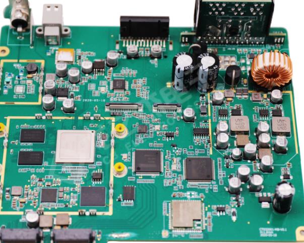
Circuit board

(2) Metal and ceramic packaging shells, gold wire and wafer bonding data;
(3) Permeable materials, such as molding compound and silicon;
(4) Defects such as voids, cracks and PCB through-hole When the X-ray passes through the first and second class data, the X-ray passes less, and the resulting image has a higher gray value; When the X-ray passes through the third type, the obtained image has a lower gray value; The fourth type, X - ray completely penetrates and finally becomes a bright image
X ray
The 2D X-ray detector can be tilted at an angle of ± 70 ° First, adjust the voltage, and adjust the power and contrast of the X-ray detector to achieve the best image quality The whole detection process is mainly divided into four steps, which is also called 3+1 method in this paper
(1) Carry out global inspection on PCB, mainly including PCB and components;
(2) Enlarge the image for local inspection to find defects or suspicious defects;
(3) Identify, analyze and confirm suspicious defects through re amplification and tilt imaging;
(4) Tilt imaging shall be carried out for all BGA packaging devices to preliminarily check whether the solder joints are defective.
At present, it is difficult to solve the problem of detecting invisible welding defects in polychlorinated biphenyls Based on the 2D X-ray detector, the detection method and process are proposed The X - ray testing scheme is verified by experiments. The results show that the X - ray testing scheme is reasonable and feasible According to this inspection scheme, PCBs with common welding defects can be identified, which can also guide PCB design and welding process improvement X-ray inspection program has the following advantages during inspection: clear imaging, easy to identify defects; Common defects covered by polychlorinated biphenyls, with high work quality; Standardized operation procedure, high detection efficiency
Strict control of product quality is not only the embodiment of high-quality production services provided by enterprises, but also a favorable guarantee for industrial safety production. Strengthening the quality inspection of castings and ensuring the production quality is the key to ensure the sustainable development of China's manufacturing industry.
Composition and function of SMT head
Dec 02,2022


Just upload Gerber files, BOM files and design files, and the KINGFORD team will provide a complete quotation within 24h.