
Professional PCB manufacturing and assembly
Building 6, Zone 3, Yuekang Road,Bao'an District, Shenzhen, China
+86-13410863085Mon.-Sat.08:00-20:00


What are the proofing requirements in SMT chip processing
In the electronic industry, the personnel involved in SMT chip proofing process are very important Printed circuit board, printed circuit board, is widely used as the basis of electronic circuits Printed circuit boards are used to provide a mechanical basis on which circuits can be built In retrospect, almost all printed circuit boards and their designs used for circuits are used by millions of people
Although today's PCBs form the basis of almost all electronic circuits, they are usually taken for granted However, science and technology in this area are progressing The track size is reduced, and the number of layers in the circuit board is being added to adapt to the new connections required. The design rules are being improved to ensure that smaller SMT equipment can handle and adapt to the welding process used in production
Process requirements for SMT chip protection
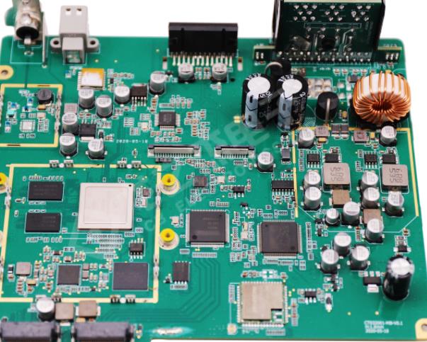
Circuit board

Process requirements for SMT chip protection and placement of components The installed components shall be accurately placed on the printed circuit board one by one according to the requirements of the assembly drawing and the assembly board schedule 1. SMT processing and placement process requirements The nominal value and polarity of each assembly number component on the type, model and circuit board must meet the requirements of the product assembly drawing and the list
The installed components must be intact.
The thickness of the solder end or solder foot of the smt wafer mounting assembly immersed in the solder paste shall not be less than 1/2. For general parts, the solder paste extrusion amount during placement shall be less than 0.2mm, and for fine pitch parts, the solder paste extrusion amount during placement shall be less than 0.1mm.
The welding end or leg of the assembly shall be aligned and centered with the weld ring pattern. Due to the self-aligning effect of reflow soldering, a certain deviation is allowed during component installation. Refer to relevant IPC standards for specific deviation range of each component.
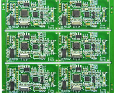
The PCB manufacturing process can be implemented in many ways and has many variations. Although there are many small changes, the main stages in the SMT chip proofing manufacturing process are the same.
Printed circuit board, printed circuit board, can be made of various substances. The most widely used fiberglass substrate is called FR4. This provides a reasonable degree of stability under temperature changes. Although the cost is not too high, it is not as serious as the failure. Other cheaper materials can be used for printed circuit boards in low-cost commercial products. For high-performance RF design, the dielectric constant of the substrate is very important. Low loss is required, and then PTFE based printed circuit boards can be used, although they are more difficult to handle.
In order to form a track with the components in PCB, first obtain the copper clad plate This includes the substrate, usually FR4, and the usual copper cladding on both sides The copper coating is attached to a thin layer of copper on the motherboard This combination is usually very suitable for FR4, but the nature of PTFE makes this more difficult, which adds PTFE PCB processing


Just upload Gerber files, BOM files and design files, and the KINGFORD team will provide a complete quotation within 24h.