
Professional PCB manufacturing and assembly
Building 6, Zone 3, Yuekang Road,Bao'an District, Shenzhen, China
+86-13410863085Mon.-Sat.08:00-20:00

PCB Factory: How many FPC types and processes do you know?
PCB manufacturers, PCB designers and PCBA manufacturers will explain to you: PCB manufacturers: how many FPC types and processes do you know?
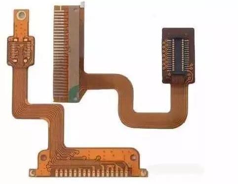
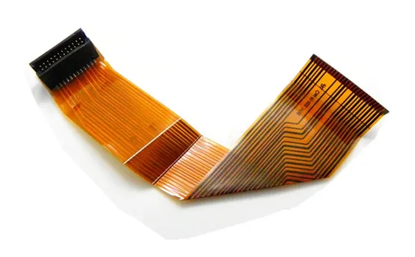
What is FPC
Flexible circuit board is a highly reliable and excellent flexible printed circuit board made of polyimide or polyester film. It is called soft board or FPC for short.
Features: High wiring density, light weight and thin thickness; It is mainly used in mobile phones, laptops, PDAs, digital cameras, LCMs and many other products.
Type of FPC
1 Single layer FPC
The conductive pattern layer on the flexible insulating substrate is calendered copper foil. The insulating substrate can be polyimide, polyethylene terephthalate, aramid fiber ester and polyvinyl chloride. Single layer FPC can be divided into the following four sub categories:
1. Single side connection without covering layer
The wire pattern is on the insulating substrate, and there is no covering layer on the wire surface. Its interconnection is realized by tin welding, fusion welding or pressure welding, which is commonly used in early telephone sets.
2. Single side connection with covering layer
Compared with the former type, only a layer of covering layer is added on the surface of the conductor. The pad shall be exposed when covering, and it can be simply not covered in the end area. It is one of the most widely used single-sided soft PCBs, used in automotive instruments and electronic instruments.
3. Double sided connection without overlay
The connection panel interface can be connected on the front and back of the wire. A passage hole can be opened on the insulating substrate at the bonding pad. This passage hole can be punched, etched or made by other mechanical methods on the required position of the insulating substrate.
4. Overlay double-sided connection
At the difference of the former type, there is a covering layer on the surface with access holes, which allows both sides of the covering layer to be terminated, and the covering layer is still maintained, which is made of two layers of insulating materials and one layer of metal conductor.
2 Double sided FPC
The double-sided FPC has a conductive pattern made of etching on both sides of the insulating base film, which increases the wiring density per unit area. The metallized hole connects the figures on both sides of the insulating material to form a conductive path to meet the design and use functions of flexibility. The covering film can protect the single and double sided wires and indicate the location of the components. As required, metallized holes and coatings are optional, and this type of FPC is rarely used.
3 Multilayer FPC
Multilayer FPC refers to laminating three or more layers of single-sided or double-sided flexible circuits together, forming metallized holes by drilling and electroplating, and forming conductive paths between different layers. In this way, complex welding processes are not required. Multilayer circuits have huge functional differences in terms of higher reliability, better thermal conductivity and more convenient assembly performance.
Its advantages are light weight of the substrate film and excellent electrical properties, such as low dielectric constant. Multilayer flexible PCB board made of polyimide film is about 1/3 lighter than rigid epoxy glass cloth multilayer PCB board, but it loses the excellent flexibility of single-sided and double-sided flexible PCB. Most of these products do not require flexibility. Multilayer FPC can be further divided into the following types:
1. Finished flexible insulating substrate
This type is made on flexible insulating substrate, and the finished product is specified as flexible. This structure usually bonds the two ends of many single-sided or double-sided microstrip flexible PCB together, but their center parts are not bonded together, so that they are highly flexible. In order to have high flexibility, a thin and suitable coating, such as polyimide, can be used on the conductor layer to replace a thick laminated coating.
2. Finished soft insulating substrate
This type is made on flexible insulating substrate, and the finished products can be flexed as specified. This kind of multilayer FPC is made of flexible insulating materials, such as polyimide film, laminated into multilayer boards, which lose their inherent flexibility after lamination.
FPC manufacturing process
Up to now, almost all FPC manufacturing processes are processed by subtractive method (etching method). Generally, copper clad foil is used as the starting material to form an anti-corrosive layer by photolithography, and the circuit conductor is formed by etching to remove some copper surfaces. Due to the side etching and other problems, the etching method has the processing limitation of micro circuits.
Based on the fact that the subtractive method is difficult to process or maintain high qualification rate microcircuits, people think that the semi additive method is an effective method, and people have proposed various semi additive methods. An example of the fabrication of the microcircuit using semi addition method. The semi addition process takes polyimide film as the starting material. First, the liquid polyimide resin is cast (coated) on an appropriate carrier to form a polyimide film.
Next, the sputter method is used to form the planting layer on the polyimide substrate film, and then the photolithography method is used to form the anti corrosion layer pattern of the inverse pattern of the circuit on the planting layer, which is called the resistant coating. The blank part is plated to form a conductor circuit. Then, the anti erosion layer and unnecessary crystal planting layer are removed to form the first layer of circuit. A photosensitive polyimide resin is coated on the first layer of circuit, and holes, protective layers or insulating layers for the second layer of circuit are formed by photolithography, and then a planting layer is sputtered on the first layer to form a substrate conductive layer for the second layer of circuit. The multilayer circuit can be formed by repeating the above process.
Using this half addition method, the submicron circuit with a pitch of 5 um and a through hole of 10 um can be fabricated. The key of making ultramicro circuits by semi addition method is the performance of the photosensitive polyimide resin used as insulating layer. PCB manufacturers, PCB designers and PCBA manufacturers will explain to you: PCB manufacturers: how many FPC types and processes do you know?


Just upload Gerber files, BOM files and design files, and the KINGFORD team will provide a complete quotation within 24h.