
Professional PCB manufacturing and assembly
Building 6, Zone 3, Yuekang Road,Bao'an District, Shenzhen, China
+86-13410863085Mon.-Sat.08:00-20:00

Advantages of PCB Reserved Process Edge and Selection of Substrate Materials
PCB manufacturing, PCB design and PCBA processing manufacturers explain the advantages of PCB reservation process and the selection of substrate materials
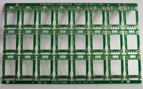
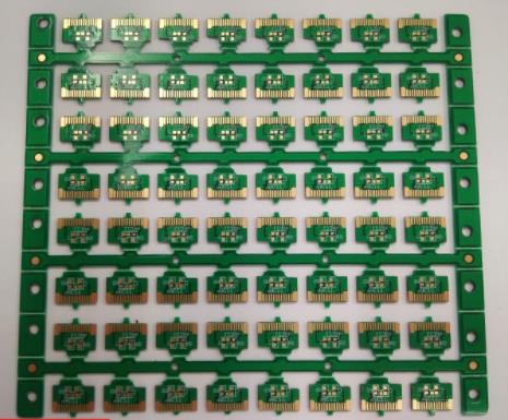
In the PCB production process flow, the process edge reservation is of great significance for the subsequent SMT chip processing. The process edge is to assist the SMT plug-in to weld the added parts of the walking board on both sides or four sides of the PCB board, mainly to assist production. It is not a part of the PCB board and can be removed after PCBA manufacturing and production.
Since the process side will consume more PCB boards, which will increase the overall cost of PCB, it is necessary to balance economy and manufacturability when designing PCB process side. For some PCB boards with special shapes, the original PCB boards with 2 or 4 process edges can be greatly simplified through panel assembly. The track width of SMT mounter shall be fully considered when designing the panel assembly method during the patch processing. For the panel assembly exceeding 350mm in width, it is necessary to communicate with the process engineer of SMT supplier.

The main reason for leaving the process edge is that the SMT mounter track is used to clamp the PCB board and flow through the mounter. Therefore, components too close to the track edge will collide with each other when the SMT mounter nozzle absorbs the components and pastes them onto the PCB board. Therefore, a certain process edge must be reserved, such as 2-5mm. Similarly, it is also applicable to some plug-in components to prevent similar phenomena during wave soldering.
The flatness of PCB production process edge is also an important part of PCB production. When removing the process edge of PCB production, it is necessary to ensure that the process edge is flat. Especially for PCB boards with extremely high assembly accuracy requirements, any uneven burrs will lead to the offset of the installation hole position, which will cause great trouble for subsequent PCBA assembly.
Precautions for PCB substrate material selection
1. The base material with high glass transition temperature shall be properly selected, and Tg shall be higher than the circuit operating temperature. Tg is glass transition temperature, namely melting point; The circuit board must be flame resistant, cannot burn at a certain temperature, and can only be softened. The temperature point at this time is called glass transition temperature (Tg point), which is related to the dimensional durability of PCB.
2. The selected plate shall have high heat resistance and good flatness. It is generally required that PCB board shall have heat resistance of 250 ℃/50S.
3. In terms of electrical performance, it is required to select materials with high dielectric constant and low dielectric loss for high frequency circuits, including insulation resistance, voltage withstand strength and arc resistance, which should meet the product requirements, especially the low thermal expansion coefficient.
4. General electronic products adopt FR4 epoxy glass fiber substrate; Polyimide glass fiber substrate shall be used for high ambient temperature or flexible circuit board; For high-frequency board, PTFE glass fiber substrate is required; For electronic products with high heat dissipation requirements, metal substrate shall be used. PCB manufacturing, PCB design and PCBA processing manufacturers will explain the advantages of PCB reservation process and the selection of substrate materials.


Just upload Gerber files, BOM files and design files, and the KINGFORD team will provide a complete quotation within 24h.