
Professional PCB manufacturing and assembly
Building 6, Zone 3, Yuekang Road,Bao'an District, Shenzhen, China
+86-13410863085Mon.-Sat.08:00-20:00

Computer motherboard - manufacturing of multilayer PCB printed circuit board
Circuit board manufacturing, circuit board design and PCBA processing manufacturers will explain the manufacturing of computer motherboards - multilayer PCB printed circuit boards.
In 1936, Austrian Paul Eisler first used printed circuit boards in radios. In 1943, most Americans used this technology in military radios. In 1948, the United States officially recognized that this invention could be used for commercial purposes. Since the mid 1950s, PCB has been widely used.
Before the emergence of PCB, the interconnection between electronic components was completed by direct wire connection. Nowadays, wires are only used for laboratory test applications; Printed circuit board has definitely occupied the position of absolute control in the electronic industry.
In order to increase the area that can be wired, more single and double sided wiring boards are used for multilayer boards. A printed circuit board with one double-sided as the inner layer, two single-sided as the outer layer, or two double-sided as the inner layer, and two single-sided as the outer layer, is a four layer or six layer printed circuit board, also known as a multilayer printed circuit board, when the positioning system and insulating bonding materials are alternately combined and the conductive patterns are interconnected according to the design requirements.
Copper clad laminate is the substrate material for making printed circuit boards. It is used to support various components and can realize electrical connection or electrical insulation between them.
From the beginning of the 20th century to the end of the 1940s, a large number of resins, reinforcement materials and insulating substrates for substrate materials emerged, and the technology was initially explored. All these have created the necessary conditions for the emergence and development of the most typical substrate material for printed circuit boards - copper clad laminate. On the other hand, PCB manufacturing technology with metal foil etching (subtraction) as the mainstream has been initially established and developed. It plays a decisive role in determining the structural composition and characteristic conditions of CCL.
In printed circuit boards, lamination is also known as "lamination". It is used to laminated the inner monoliths, semi solidified sheets and copper foils together to form multilayer boards at high temperature. For example, a four layer board needs to be made by pressing one inner single sheet, two copper foils and two sets of semi solidified sheets.
The drilling process of multilayer PCB is generally not completed at one time, which is divided into one drill and two drills.
The first drill requires the copper sinking process, that is, the hole is plated with copper so that the upper and lower layers can be connected, such as through holes, original holes, etc.
The second drill holes are those that do not need copper, such as screw holes, positioning holes, heat sink, etc. The inner pockets of these holes do not need copper.
Film is an exposed negative. The PCB surface will be coated with a layer of photosensitive liquid, which will be dried after a temperature test of 80 ° C, and then pasted on the PCB board with film. Then, the film will be exposed by an ultraviolet exposure machine, and the film will be torn off. The circuit diagram is displayed on the PCB.
Green oil refers to the ink coated on the copper foil on the PCB. This layer of ink can cover conductors other than pads, avoid welding short circuit, and extend the service life of the PCB during use; It is generally called resistance welding or anti welding; The colors are green, black, red, blue, yellow, white, matt, etc. Most PCBs use green solder resist ink, which is commonly called green oil;
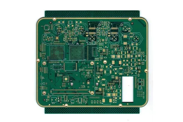
The plane of the computer motherboard is a PCB (printed circuit board), which generally uses four or six layers of boards. Relatively speaking, in order to save costs, low-grade motherboards are mostly four layers: the main signal layer, the ground layer, the power supply layer, and the secondary signal layer, while six layers of boards add the auxiliary power supply layer and the medium signal layer. Therefore, the motherboard of six layers of PCBs is more resistant to electromagnetic interference, and the motherboard is more stable.
Circuit board manufacturing, circuit board design and PCBA processing manufacturers will explain the manufacturing of computer motherboards - multilayer PCB printed circuit boards.


Just upload Gerber files, BOM files and design files, and the KINGFORD team will provide a complete quotation within 24h.