
Professional PCB manufacturing and assembly
Building 6, Zone 3, Yuekang Road,Bao'an District, Shenzhen, China
+86-13410863085Mon.-Sat.08:00-20:00

PCB proofing process may encounter various problems. As a PCB proofing manufacturer, you need to pay attention to various situations in the process:
1) The distance from the edge of the pad hole to the edge of the PCB board for pcb proofing is greater than 1mm, which can avoid the defects of the welding plate during processing.
Precautions for pcb proofing are as follows:
1) The distance from the edge of the pad hole to the edge of the PCB board for pcb proofing is greater than 1mm, which can avoid the defects of the welding plate during processing.
2) The bonding pad is torn. When the copper film wire connected to the bonding pad is thin, the connection between the bonding pad and the copper film wire should be designed as a teardrop, so that the bonding pad is not easy to peel off, and the copper film wire and the wire between the connections are not easy to disconnect.
3) Adjacent pads shall avoid sharp corners.
The purpose of large-area filling on the PCB board is two, one is to dissipate heat, the other is to reduce shielding interference. The pcb is sampled to avoid the heat generated during the process, so that there is no discharge of the gas generated by the circuit board and the copper film falls off. It should be filled on a large area of the window, which makes the filler mesh.
The use of copper can also achieve the purpose of anti-interference. Copper can automatically bypass the PCB pad and can be connected to the ground wire.
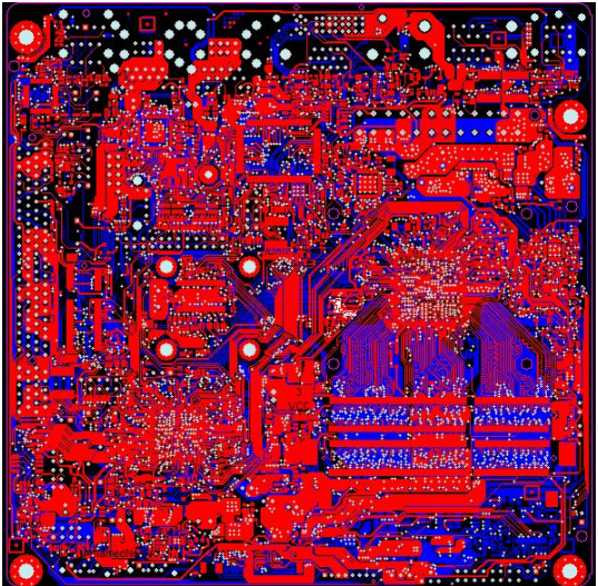
Cross wiring of PCB board In the design of single sided PCB board, when some copper films cannot be connected, the common practice is to use cross wiring, and the cross wiring length should be selected as follows: 6mm, 8mm and 10mm.
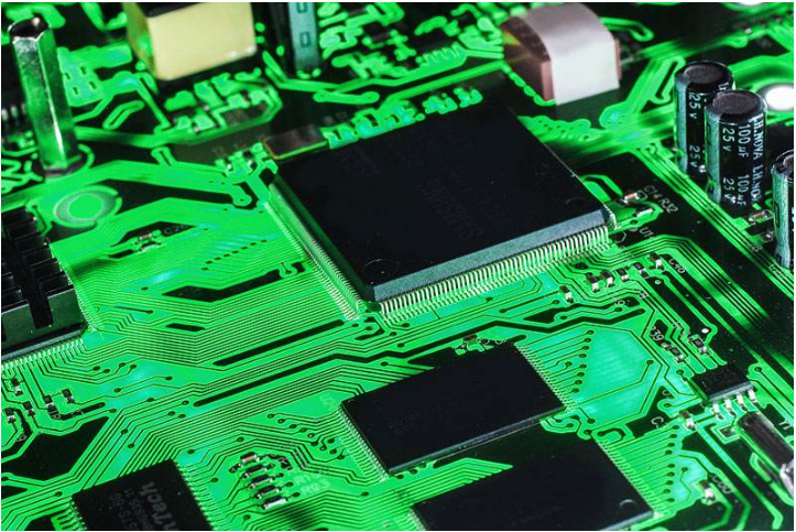
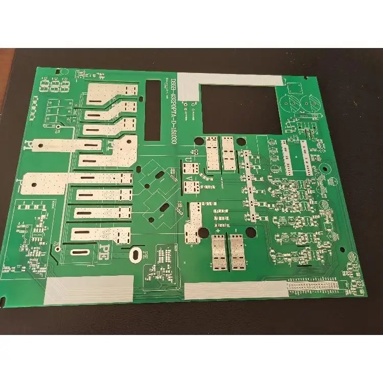
PCB proofing
High frequency wiring of PCB board
In order to make the design of high-frequency PCB more reasonable and better anti-interference performance, the following aspects should be considered in PCB design:
1) Reasonable selection of layers for pcb proofing
The middle inner plane is used as the power supply and ground plane, which can play a shielding role, effectively reduce the parasitic inductance, shorten the signal line length, and reduce the cross interference between signals. Generally speaking, the noise of the four layer board is 20 dB lower than that of the two layer board.
2) Pcb proofing travel line mode
The wiring must be rotated at an angle of 45 °, which can reduce the transmission of high-frequency signals and mutual coupling.
3) Pcb proofing wiring length
The shorter the line length, the better. The shorter the parallel distance between two lines, the better.
4) Number of holes
The fewer the holes, the better.
5) Mezzanine wiring direction
When pcb proofing, the inter layer wiring direction should be vertical, that is, the top layer is horizontal and the bottom is vertical, which can reduce the interference between signals.
6) Copper coating
Adding grounding copper coating can reduce the interference between signals.
7) Parcel place
The grouping processing of important signal lines for pcb proofing can significantly improve the anti-interference ability of signals. Of course, the interference source can be wrapped so that it will not interfere with other signals.
8) Signal cable
The signal wiring cannot be cycled, and it needs to be wired according to the daisy chain mode. Shenzhen is the city that produces the most pcb boards in China, and what are the pcb proofing companies?
9) Decoupling capacitor
The cross decoupling capacitor is connected to the power supply end of the integrated circuit.
10) Digital, analog and other high frequency choke coils are connected to the common ground wire and connected to the high frequency choke device. The pcb proofing is generally through the center hole of the high frequency ferrite beads and wires.


Just upload Gerber files, BOM files and design files, and the KINGFORD team will provide a complete quotation within 24h.