
Professional PCB manufacturing and assembly
Building 6, Zone 3, Yuekang Road,Bao'an District, Shenzhen, China
+86-13410863085Mon.-Sat.08:00-20:00


Introduction to PCB board leveling electroplating technology
1、 Overview
With the rapid development of microelectronics technology, the manufacturing of PCB is developing rapidly in the direction of multi-level, stacking, functionalization, and integration It promotes the design and design of circuit patterns using small holes, narrow spacing, and thin lines in printed circuit design, which makes the manufacturing technology of printed circuit boardsmore difficult. Especially because the aspect ratio of through holes in multilayer boards exceeds 5:1, and the deep blind holes widely used in products, the traditional vertical electroplating process cannot meet the scientific and technological requirements of high quality and high reliability interconnection holes The main reason is to analyze the current distribution state from the electroplating principle During the actual electroplating, it was found that the current distribution in the hole was waist drum shaped. From the edge of the hole to the center of the hole, the current distribution in the hole gradually decreased, resulting in a large amount of copper deposition on the surface and hole At the edge of the hole, in the center of the hole where copper is required, it is impossible to ensure the standard thickness of the copper layer Sometimes the copper layer is very thin or there is no copper layer In serious cases, this will cause irreparable losses, leading to a large number of multi-layer wall scrap In order to solve the problem of product quality in mass production, at present, the problem of deep hole electroplating has been solved from two aspects of current and additives Most copper plating processes for high aspect ratio printed circuit boards are carried out under relatively low current density with the aid of high-quality additives, moderate air stirring and cathode movement The effect of electroplating additive can only be shown by the electrode reaction control area in the newly added hole In addition, the cathode movement is conducive to improving the deep plating capacity of the plating solution, and the polarization of the plating part is increased The formation rate of the crystal nucleus and the growth rate of the crystal grains compensate each other to obtain a high toughness copper layer However, when the aspect ratio of through-hole continues to increase or deep blind holes appear, these two process measures become ineffective, resulting in a level electroplating technology It is a continuation of the development of vertical electroplating technology, that is, a new electroplating technology based on vertical electroplating technology The key of this technology is to establish a mutually compatible horizontal electroplating system. By improving the coordination of power supply pipelines and other auxiliary equipment, the highly dispersed electroplating solution is superior to the vertical electroplating method
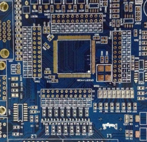
PCB board

2. Introduction to the principle of leveling electroplating
The method and principle of horizontal electroplating and vertical electroplating are the same, both of which must have cathode and anode. After electrification, electrode reaction occurs to ionize the main components of the electrolyte, so that the charged positive ions move to the negative phase of the electrode reaction zone; Charged negative ions move towards the electrode. The positive phase shift in the reaction zone then produces a metal deposition coating and outgassing. Because the deposition process of metal at the cathode is divided into three steps: namely, the hydrated ions of metal diffuse to the cathode; The second step is that metal hydrated ions gradually dehydrate and adsorb on the cathode surface when passing through the double electric layer; The first step is that the metal ions adsorbed on the cathode surface receive electrons and enter the metal lattice. The actual observation of the working tank is an unobservable heterogeneous electron transfer reaction between the solid electrode and the interface of the liquid plating solution. Its structure can be explained by the double electric layer principle in electroplating theory. When the electrode is a cathode and in a polarized state, due to electrostatic force, cations with positive charges are arranged on the cathode in an orderly pipeline around the water molecules. Nearby, the phase plane formed by the cation center near the cathode is called the Helmholtz outer layer, and the distance between the outer layer and the electrode is about 1-10 nm. However, due to the total positive charge carried by the outer cation of Helmholtz, the positive charge is not enough to neutralize the negative charge on the cathode. The solution far from the cathode is affected by convection, and the concentration of cations in the solution layer is higher than that of anions. Because of electrostatic force, this layer is smaller than the outer layer of Helmholtz, and is also affected by thermal movement. The cation arrangement is not as compact and neat as Helmholtz's outer layer. This layer is called diffusion layer. The thickness of the diffusion layer is inversely proportional to the flow rate of the bath. In other words, the faster the bath flow rate is, the thinner the diffusion layer is, and vice versa. Generally, the thickness of the diffusion layer is about 5-50 microns. It is far from the cathode, and the bath layer reached by convection is called the main bath. Because the convection generated by the solution will affect the uniformity of the bath concentration. Copper ions in the diffusion layer are transferred to the outer Helmholtz layer through diffusion and ion migration in the bath. Copper ions in the main tank are transferred to the cathode surface through convection and ion migration. In the process of leveling electroplating, copper ions in the bath are transferred to the cathode in three ways to form a double electric layer.
Convection of electroplating solution is caused by external and internal mechanical agitation and pump agitation, swing or rotation of electrode itself and flow of electroplating solution caused by temperature difference. The closer to the surface of the solid electrode, the slower the flow of the electroplating solution becomes due to its friction resistance. At this time, the convection velocity on the surface of the solid electrode is zero. The rate gradient layer formed from the electrode surface to the convection bath is called the flow interface layer. The thickness of the flow interface layer is about ten times that of the diffusion layer, and the ion transport in this diffusion layer is almost not affected by convection. Under the action of electric field, ions in electroplating solution are affected by electrostatic force, resulting in ion migration, which is called ion migration. The migration rate is expressed as: u=zeon/6 Ï Ì r Î to. Where u is the ion migration rate, z is the charge number of ions, the charge of electrons (i.e. 1.61019C), E is the potential, r is the radius of hydrated ions, and η·· is the viscosity of the electroplating solution. According to the calculation of the equation, the larger the potential drop E is, the smaller the viscosity of the electroplating solution is, and the faster the ion migration speed is.
According to the electrodeposition theory, in the electroplating process, the printed circuit board on the cathode is a non ideal polarized electrode. The copper ions adsorbed on the cathode surface obtain electrons and are reduced to copper atoms, thus increasing the concentration of copper ions close to the cathode. Reduce this and form a copper ion concentration gradient near the cathode. The bath layer with copper ion concentration lower than that of the main bath is the diffusion layer of the bath. However, the copper ion concentration in the main plating solution is relatively high, which will diffuse to the places near the cathode where the copper ion concentration is low, and constantly supplement the cathode area. A printed circuit board is similar to a flat cathode. The relationship between the current size and the thickness of the diffusion layer is the COTTRELL equation: where I is the current, z is the charge number of copper ions, F is the Faraday constant, a is the cathode surface area, D is the diffusion coefficient of copper ions (D=KT/6 Ï Ì Ì Ì Ì r Ì ·), Cb is the concentration of copper ions in the main tank, Co is the concentration of copper ions on the cathode surface, D is the thickness of the diffusion layer, K is the Portman constant (K=R/N), and T is the temperature, R is the radius of hydrated copper ion, and Î is the viscosity of electroplating solution. When the copper ion concentration on the cathode surface is zero, the current is called the limiting diffusion current ii:
It can be seen from the above formula that the limit diffusion current is determined by the concentration of copper ions in the main bath, the diffusion coefficient of copper ions and the thickness of the diffusion layer. When the concentration of copper ions in the main bath is high, the diffusion coefficient of copper ions is large, the diffusion layer is thin, and the limiting diffusion current is large.
According to the above formula, in order to reach a higher limit current value, appropriate scientific and technological measures must be taken, namely heating technology. Since the diffusion coefficient can be increased by increasing the temperature, the new convection velocity can make it eddy and obtain a thin and uniform diffusion layer. From the above theoretical analysis, it can be seen that increasing the concentration of copper ions in the main bath, increasing the bath temperature and increasing the convection speed can increase the limit diffusion current to accelerate the plating speed. The horizontal electroplating is based on the eddy current formed by the accelerated convection velocity of the electroplating solution, which can effectively reduce the thickness of the diffusion layer to about 10 microns. In this case, the current density can be as high as 8A/dm2 when the level electroplating system is used for electroplating. The key of PCB electroplating is how to ensure the uniformity of copper layer thickness on both sides of the substrate and the inner wall of the through hole. In order to obtain the uniformity of coating thickness, it is necessary to ensure that the flow rate of plating solution on both sides of the printed board and in the through hole is fast and consistent, so as to obtain a thin and uniform diffusion layer. In order to obtain a thin and uniform diffusion layer, according to the structure of the current level electroplating system, although many nozzles are installed in the system, the plating solution can be rapidly and vertically sprayed onto the printed board to accelerate the flow of the plating solution in the through-hole. The flow rate of the plating solution is very fast, forming eddy currents in the upper and lower sides of the substrate and through holes, thereby reducing the diffusion layer and making it more uniform. However, when the plating solution suddenly flows into the narrow through-hole, the plating solution at the inlet of the through-hole will also appear reverse reflux. Combined with the influence of current distribution, this phenomenon usually leads to electroplated holes at the inlet. The copper layer is too thick due to this effect, and a dog bone like copper coating is formed on the inner wall of the through-hole. According to the flow state of the plating solution in the through-hole, that is, the size of eddy current and reflux, and the analysis of the quality of the conductive plating through-hole, the control parameters can only be determined through the process testing method to achieve the uniformity of the coating thickness of the printed circuit board. Since the size of eddy current and reflux is still unknown through theoretical calculation, only the measurement process method is used. It can be seen from the measurement results that, in order to control the uniformity of the copper coating thickness of the through-hole, it is necessary to adjust the controllable process parameters according to the aspect ratio of the through-hole of the printed circuit board, or even select a highly dispersive copper plating solution, and then add appropriate additives to improve the power supply pipeline, that is, use reverse pulse current for electroplating to obtain a copper coating with strong distribution capacity. Especially, with the increase of the number of micro blind holes in the laminate, not only the level electroplating system should be used for electroplating, but also ultrasonic vibration should be used to promote the replacement and recycling of the plating solution in the micro blind holes. The data can be adjusted to correct controllable parameters, and satisfactory results can be obtained.
3. Basic structure of leveling electroplating system
According to the characteristics of horizontal electroplating, the placement pipeline of printed circuit board was changed from vertical electroplating to parallel electroplating. At this time, the printed circuit board is the cathode, and some leveling electroplating systems use conductive clips and conductive rollers to provide current. From the convenience of the operating system, it is more common to use the roll conduction supply method. In addition to being the cathode, the conductive roller in the leveling electroplating system also has the function of conveying the printed circuit board. Each conductive roller is equipped with a spring device, which is designed to meet the electroplating needs of printed circuit boards with different thicknesses (0.10-5.00mm). However, during electroplating, parts in contact with the plating solution may be coated with copper, and the system cannot operate for a long time. In this case, most of the current level electroplating systems are designed to switch the cathode to the anode, and then use a group of auxiliary cathodes to electrolyze the copper on the electroplating roller. The new plating design also allows easy removal or replacement of wear prone areas for maintenance or replacement purposes. The anode consists of a series of insoluble titanium baskets with adjustable size. These titanium baskets are placed at the upper and lower positions of the printed circuit board and filled with spherical soluble copper with a diameter of 25 mm. The phosphorus content is 0.004-0.006%, and the distance between the cathode and the anode. 40mm. The flow of the plating solution is a system composed of a pump and a nozzle, which makes the plating solution flow rapidly in a closed plating tank, alternating back and forth, up and down, and can ensure the uniformity of the plating solution flow. The electroplating solution is vertically sprayed on the printed circuit board to form wall jet vortex on the surface of the printed circuit board. The ultimate goal is to achieve rapid flow of electroplating solution on both sides of the PCB and through holes to form eddy currents. In addition, a filter system is installed in the tank. The filter screen is 1.2 microns, which is used to filter particulate impurities generated in the electroplating process to ensure that the electroplating solution is clean and free of pollution.
In the manufacture of leveling electroplating system, the convenience of operation and automatic control of process parameters should also be considered. Because in actual electroplating, with the size of PCB, the size of through-hole diameter and the required copper thickness, the transmission rate, the distance between PCB, the size of pump horsepower, the nozzle, the direction and current density of copper and other process parameters, it is necessary to test, adjust and control to obtain the copper layer thickness that meets the scientific and technological requirements. It must be controlled by a computer. In order to improve production efficiency and the consistency and reliability of sub product quality, the pre and post processing of PCB through-hole (including electroplating through-hole) is based on the process flow, forming a complete level electroplating system, which is suitable for the development and release of new products. need
4. Development advantages of standard electroplating
The development of standard electroplating technology is not accidental, but the inevitable result of the special functional requirements for high-density, high-precision, multi-function, high aspect ratio multilayer printed circuit board products. Its advantages are that it is more advanced than the vertical rack electroplating process currently used, the product quality is more reliable, and mass production can be realized. Compared with the vertical electroplating process, it has the following advantages:
1) It can adapt to various sizes without manual installation and suspension, and can realize fully automatic operation, which is extremely conducive to improving and ensuring that the operation process will not damage the surface of the substrate, and is extremely conducive to large-scale production.
2) In the process review, there is no need to leave a clamping position, and a new practical area is added, which greatly saves the loss of raw materials.
3) The whole process of leveling electroplating is controlled by the computer. This substrate is under the same conditions to ensure the uniformity of electroplating on the surface and holes of each printed circuit board.
4) From the perspective of management, the cleaning of electroplating bath, the addition and replacement of electroplating solution can be completely automated, and the management will not be out of control due to human error.
5) It can be seen from the actual products that multi-level level cleaning is adopted for level electroplating, which greatly saves cleaning water and reduces the pressure of sewage treatment.
6) Due to the closed operation of the system, the pollution of the working space and the direct impact of heat evaporation on the process environment are reduced, and the working environment is greatly improved. Especially when baking the plates, the heat loss is reduced, unnecessary energy consumption is saved, and the production efficiency is greatly improved.
5. Summary
The emergence of standard electroplating technology is completely to meet the needs of high aspect ratio through-hole electroplating However, due to the complexity and particularity of electroplating process, there are still some technical problems in the design and development of electroplating system This needs to be improved in practice Nevertheless, the use of standard electroplating systems is a major development and progress in the printed circuit industry Because the application of this equipment in high-density multilayer board manufacturing shows great potential, it can not only save manpower and operation time, but also produce faster and more efficiently than the traditional vertical electroplating line In addition, the energy consumption, waste liquid, waste water and waste gas to be treated are reduced, the process environment and conditions are greatly improved, and the quality level of electroplating coating is improved The leveling electroplating line is suitable for 24-hour continuous operation of mass production The adjustment of horizontal electroplating line is slightly more difficult than that of vertical electroplating line After debugging, it is very stable Adjust the electroplating solution to ensure long-term stable operation of PCB


Just upload Gerber files, BOM files and design files, and the KINGFORD team will provide a complete quotation within 24h.