Analysis of Transient Signal in PCB Design
The transient response PCB board of interconnection and power line is the cause of bit error, timing jitter, and other signal integrity problems You can use transient signal analysis to determine the design steps to take when designing a perfect circuit Transient signal analysis in simple circuits can be manually checked and calculated, allowing mapping of transient responses over time More complex circuits may be difficult to analyze manually Instead, you can use the simulator for time-domain transient signal analysis during simulator design If you use the right design software, you don't even need coding skills Formally, transients may occur in circuits that can be written as a set of coupled first order linear or non-linear differential equations (autonomy or non autonomy) The transient response can be determined in several ways
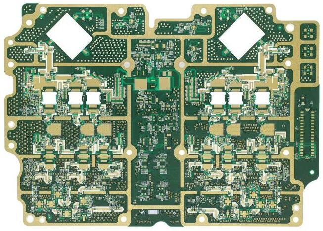
PCB board

The transient response without echo in the time invariant circuit can be divided into one of the following three cases:
1) Overdamping: slow attenuation of response, no oscillation
2) Critical damping: fast attenuation response, no oscillation
3) Insufficient damping: damping oscillation response
For circuit simulation, transient signal analysis simulation can be run directly from the schematic diagram. Two aspects of circuit behavior need to be considered:
1) Drive signal. This defines the change in the input voltage/current level that results in a transient response. This may involve a change between two signal levels (i.e. switching digital signals), a drop or spike in the current input signal level, or any other arbitrary change in the drive signal. You can consider driving with a sinusoidal signal or any periodic waveform. You can also consider the limited rise time of the signal when switching between two levels.
2) Initial conditions. This defines the state of the circuit when the drive signal fluctuates or the drive waveform is turned on. Assume that at time t=0, the circuit is initially in steady state (i.e., there is no previous transient response in the circuit). If no initial conditions are specified, the voltage and current are assumed to be zero at t=0. After running the analogy, you will get an output that covers the input signal and output, so that you can accurately see how different changes in signal levels produce transient responses. An example of switching digital signals is shown below. In this circuit, we assume that no initial conditions are specified. Due to insufficient damping, the transient response of the current shows severe overshoot and undershoot. One solution here is to add some series resistors at the source to add damping. A better solution is to reduce the inductance or add capacitance in the circuit to make the response enter the damping state.
Transient signal analysis after schematic diagram and layout
The output is similar to the output in the reflection waveform analogy, where the incident wave and the reflected wave are compared in the post layout analogy. In this case, the difference is that we are designing a schematic diagram that does not consider the parasitic effect in PCB. In the post layout analogy, parasitic effects are considered. The transient signal analysis results may inform you to make some changes to the layout or stack to reduce the above ringing. If the above results are seen in the signal integrity simulation after the transmission line layout, one solution is to reduce the loop inductance and capacitance in the interconnection. This will add damping to the circuit without changing the characteristic impedance. This also moves the resonant frequency in the circuit to a higher value, thereby reducing the ringing amplitude. Another option is to terminate in series at the drive.
Pole zero analysis
Another method of time-domain analogy is to use pole zero analysis. This technology brings the circuit into the Laplace domain and calculates the poles and zeros in the circuit. This allows you to immediately see the behavior of the transient signal response in the circuit. Please note that this analogy can still take into account the initial conditions in the transient signal analysis. This result is more general. However, you cannot directly see the magnitude of the transient signal because you have not explicitly considered the behavior of the input waveform.
Stability and Instability in Transient Signal Analysis
It should be noted here that there may be instability in circuits containing reverberation In a typical circuit, you will check the PCB schematic and layout, and you will almost always encounter stable transients The example above shows a steady response Although there is transient oscillation, the signal eventually attenuates to a stable state In circuits with strong reverberation, transient oscillations become unstable and grow over time Amplifier is a well-known case. In the case of strong echo, thermal fluctuation or strong underdamping response will cause the response of amplifier to become unstable and saturated The saturated nonlinear time invariant circuit will eventually force the unstable amplitude to stabilize to a constant level Transient signal analysis, you can easily find the instability in the time domain; This will occur in the underdamped state as the output index increases In pole zero analysis, the real part is the active PCB


