

Multilayer impedance control pcb board
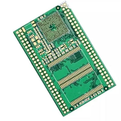
Name: Multilayer impedance control pcb board
Type: Multilayer PCB
Maximum layers: 48L
PCB thickness: 0.2-6.5mm
Finished size: 24.5*47 inches
Maximum Base Copper Weight: 12 oz
Minimum tracking/spacing: 2/2mil
Maximum PCB aspect ratio: 20:1
Minimum BGA pitch: 0.35mm
Minimum Impedance Tolerance: ±8%
PCB impedance control
There will be various signal transmission in the conductor in the circuit board. When the transmission rate is increased, the frequency must be increased. If the line itself is different due to erosion, stacking thickness, and wire width, it will cause impedance to change and make them make it. Signal distortion. Therefore, the conductor on the high -speed line board should be controlled within a certain range, called "impedance control".
The factors that affect the impedance of the PCB line are the width of the copper line, the thickness of the copper line, the dielectric constant of the medium, the thickness of the medium, the thickness of the pads, the path of the ground line, and the wiring around the line. Therefore, when designing PCB, we must control the impedance of the wiring on the board in order to avoid the reflection of the signal and other electromagnetic interference and signal integrity as much as possible to ensure the actual use of the PCB board.
Name: Multilayer impedance control pcb board
Type: Multilayer PCB
Maximum layers: 48L
PCB thickness: 0.2-6.5mm
Finished size: 24.5*47 inches
Maximum Base Copper Weight: 12 oz
Minimum tracking/spacing: 2/2mil
Maximum PCB aspect ratio: 20:1
Minimum BGA pitch: 0.35mm
Minimum Impedance Tolerance: ±8%
- Previous:Ten-layer HDI Impedance Control Automotive Digital PCB
- Next:No
