

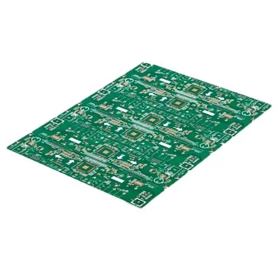
Fr4 Electronic Impedance Control PCB
Name: Fr4 Electronic Impedance Control PCB
Model: printed circuit board
Substrate: FR-4
Copper Thickness: 0.5-40Z
Plate thickness: 0.4T-4.0T
Surface Treatment: HASL, OSP, Immersion Gold/Gold
Board size: 10*1200MM
Layers: 1-20 layers
Solder mask: green. Red. blue. white. black.yellow
Size: 10-1200MM
Circuit board testing: 100% electronic testing
Certificate: ISO/TS16949/RoHS/TS16949
Material: FR4 CEM1 CEM3 High TG
Five major factors affecting impedance
The first: medium thickness. Increasing the thickness of the medium can increase the impedance, reduce the thickness of the medium, can reduce the impedance; different semi -solidary tablets have different glue content and thickness. The thickness of its pressing is related to the flatness of the crusher and the procedure of the pressure plate; for any kind of plate used, it must obtain the thickness of the medium layer that can be produced, which is conducive to design calculations. Try tolerance is the key to the thickness control of the medium.
The second: line width, increase line width, can reduce impedance, reduce line width can increase impedance. The control requirements of the wire width can be better to achieve the gap in the impedance control requirements in the +/-10 % tolerance. The gap cannot exceed 10 %. The width is mainly controlled by etching control. In order to ensure the width of the line, according to the etching side erosion, the light drawing error, and the graphic transfer error, the engineering negatives are compensated to meet the requirements of the line width.
The third: copper thickness, reducing line thickness can increase the impedance, increase the thickness of the line can reduce the impedance; the line thickness can be controlled by graphic electroplating or using the corresponding thickness copper foil to control. The control requirements for copper thickness are evenly controlled. The bleeding block of the thin line and isolated lines is added to prevent uneven copper thickness on the line, which affects the situation where the impedance is very unevenly distributed to CS and SS surface copper distribution. To cross the board on the board to achieve the purpose of the two -sided copper thickness.
The fourth: dielectric constant, increasing the dielectric constant, can reduce impedance, reducing the dielectric constant can increase impedance. The dielectric constant is mainly controlled by materials. Different plates have different dielectric constants. It is related to the resin materials used: FR4 plates, the dielectric constant is 3.9-4.5, which will increase with the frequency of use. 3.9 to obtain high signal transmission requires high impedance values, so as to have low dielectric constants.
Fifth: Welding thickness, printed welding will reduce the external impedance. Under normal circumstances, printed welding can reduce the single -ended 2 ohm, which can reduce the differential 8 ohm, and the printed decrease value of 2 times is twice the time. When the printing is more than 3 times, the impedance value will no longer change.
Name: Fr4 Electronic Impedance Control PCB
Model: printed circuit board
Substrate: FR-4
Copper Thickness: 0.5-40Z
Plate thickness: 0.4T-4.0T
Surface Treatment: HASL, OSP, Immersion Gold/Gold
Board size: 10*1200MM
Layers: 1-20 layers
Solder mask: green. Red. blue. white. black.yellow
Size: 10-1200MM
Circuit board testing: 100% electronic testing
Certificate: ISO/TS16949/RoHS/TS16949
Material: FR4 CEM1 CEM3 High TG
- Previous:HDI Impedance Control PCB
- Next:Impedance Control Electronic PCB
