
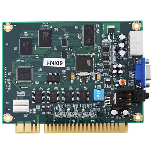
Communication equipment printed circuit board assembly
Name: Communication equipment PCB assembly
Substrate: FR-4/High TG/Polyimild/PTFE/Rogers
Copper Thickness: 1/3OZ- 6OZ
Plate thickness: 0.21-6.0mm
minute. Hole size: 0.20mm
minute. Line width: 4 million
minute. Line spacing: 0.075 mm
Surface treatment: spray tin/gold drill/OSP/lead-free spray tin
Board size: minimum 10*15mm, maximum 508*889mm
Product Type: OEM&ODM
PCB standard: IPC-A-610 D/IPC-III standard
Certificate: ISO9001/ CE//TUV/ ROHS
Warranty: 1 year
Service: One-stop turnkey service
Electronic testing: 100%
Logistics: Air/Sea
Communication equipment PCB assembly, the Chinese name is printed circuit board, also known as printed circuit board, is an important electronic component, a support for electronic components, and a carrier for electrical connections of electronic components. Because it is made using electronic printing, it is called a "printed" circuit board.

Effect
After electronic equipment adopts printed boards, due to the consistency of similar printed boards, errors in manual wiring are avoided, and automatic insertion or placement of electronic components, automatic soldering, and automatic detection can be realized to ensure the quality of electronic equipment. , Improve labor productivity, reduce costs, and facilitate maintenance.
Develop
printed circuit board assembly have developed from single-layer to double-sided, multi-layer and flexible, and still maintain their own development trends. Due to the continuous development in the direction of high precision, high density and high reliability, continuous reduction in size, cost reduction and performance improvement, printed boards still maintain strong vitality in the development of future electronic equipment.
A summary of domestic and foreign discussions on the future development trend of printed board manufacturing technology is basically the same, that is, to high density, high precision, fine aperture, thin wire, fine pitch, high reliability, multi-layer, high-speed transmission, light weight, Developing in the direction of thinness, it is also developing in the direction of improving productivity, reducing costs, reducing pollution, and adapting to multi-variety and small-batch production. The technical development level of printed circuits is generally represented by the line width, aperture, and board thickness/aperture ratio of the printed circuit board.
Source
The creator of the printed circuit board was the Austrian Paul Eisler, who first used it in a radio in 1936. In 1943, Americans mostly applied this technology to military radios. In 1948, the United States officially recognized this invention for commercial use. Printed circuit boards have only been widely used since the mid-1950s.
Before the appearance of PCB, the interconnection between electronic components was done by direct connection of wires. Today, wires exist only for experimental applications in the laboratory; printed circuit boards have definitely occupied a position of absolute control in the electronics industry.
PCB production process
Contact the manufacturer
First you need to contact the manufacturer, and then register the customer number, then someone will quote for you, place an order, and follow up the production progress.
Cutting
Purpose: According to the requirements of engineering data MI, cut the large sheets that meet the requirements into small pieces to produce sheets. Small pieces of sheet metal that meet customer requirements.
Process: large sheet → cutting according to MI requirements → curly sheet → beer fillet /edge grinding → output of the sheet
Drilling
Purpose: According to the engineering data, drill the desired hole diameter at the corresponding position on the sheet material that meets the required size.
Process: Stacking pins→upper board→drilling→lower board→inspect\repair
Immersion copper
Purpose: Immersion copper is to deposit a thin layer of copper on the wall of the insulating hole by chemical method.
Process: Coarse grinding→hanging plate→immersed copper automatic line→lower plate→immersing in % dilute H2SO4→thickened copper
Graphic transfer
Purpose: Graphic transfer is to transfer the image on the production film to the board
Process: (blue oil process): Grinding board→printing the first side→drying→printing the second side→drying→exposure→photographic→checking; (dry film process): hemp board→pressing film→standstill→pair Bit→exposure→rest→develop→check
Graphic plating
Purpose: Pattern electroplating is to electroplate a copper layer with a required thickness and a gold-nickel or tin layer with a required thickness on the exposed copper skin of the circuit pattern or on the wall of the hole.
Process: upper plate → degreasing → water washing twice → micro-etching → water washing → pickling → copper plating → water washing → pickling → tin plating → water washing → lower plate
Withdrawing the film
Purpose: Use NaOH solution to remove the anti-plating coating layer to expose the non-line copper layer.
Process: water film: insert frame → soak in alkali → rinse → scrub → pass machine; dry film: put board → pass machine
Etching
Purpose: Etching is to use chemical reaction method to corrode the copper layer of non-circuit parts.
Green oil
Purpose: Green oil is to transfer the pattern of green oil film to the board to protect the circuit and prevent tin on the circuit when welding parts
Process: grinding board→printing photosensitive green oil→curling board→exposure→developing shadow; grinding board→printing the first side→baking board→printing the second side→baking board
Characters
Purpose: Characters are provided as an easy-to-recognize mark
Process: After finishing the green oil → cooling and standing → adjusting the screen → printing characters → finishing the curium
Gilded Fingers
Purpose: Plating a layer of nickel\gold with the required thickness on the plug finger to make it more hard and wear-resistant
Process: board → degreasing → water washing twice → micro-etching → water washing twice → pickling → copper plating → water washing → nickel plating → water washing → gold plating
Tin plate (a parallel process)
Purpose: HASL is to spray a layer of lead and tin on the exposed copper surface that is not covered with solder resist oil to protect the copper surface from corrosion and oxidation, so as to ensure good soldering performance.
Process: micro-etching → air drying → preheating → rosin coating → solder coating → hot air leveling → air cooling → washing and air drying
Forming
Purpose: Through mold stamping or CNC machine tools to form the shape required by customers. Organic gongs, beer boards, hand gongs, and hand-cut
Explanation: The accuracy of the data gong machine board and the beer board is higher, followed by the hand gong, and the hand-cut board can only make some simple shapes.
Test
Purpose: Through 100% electronic testing, detect defects that affect functionality such as open circuits and short circuits that are difficult to detect visually.
Process: upper mold → board placement → test → qualified → FQC visual inspection → unqualified → repair → return test → OK → REJ → scrap
Final Inspection
Purpose: Through 100% visual inspection of board appearance defects, and repair minor defects, to avoid outflow of problematic and defective boards.
Specific workflow: Incoming material→checking data→visual inspection→qualified→FQA spot check→qualified→packing→unqualified→processing→check OK
Industry Trends
The PCB industry is developing rapidly
Since the reform and opening up, China has attracted a large-scale transfer of European and American manufacturing industries due to its preferential policies in terms of labor resources, markets, and investment. development of related industries. According to China CPCA statistics, in 2006 my country's PCB actual output reached 130 million square meters, with an output value of 12.1 billion US dollars, accounting for 24.90% of the global PCB output value, surpassing Japan to become the world's number one. From 2000 to 2006, the average annual growth rate of China's PCB market reached 20%, far exceeding the global average. The global financial crisis in 2008 had a huge impact on the PCB industry, but it did not cause a catastrophic blow to China's PCB industry. Stimulated by the national economic policy, China's PCB industry experienced a full recovery in 2010. In 2010, China's PCB output value reached 19.971 billion US dollars . Prismark predicts that China will maintain a compound annual growth rate of 8.10% between 2010 and 2015, which is higher than the global average growth rate of 5.40%.
Regional distribution is uneven
China's PCB industry is mainly distributed in South China and East China. The sum of the two reaches 90% of the country, and the industrial agglomeration effect is obvious. This phenomenon is mainly related to the fact that the main production bases of China's electronics industry are concentrated in the Pearl River Delta and the Yangtze River Delta.
PCB downstream application distribution
The distribution of downstream applications in China's PCB industry is shown in the figure below. Consumer electronics accounted for the highest proportion, reaching 39%, followed by computers, accounting for 22%, communications accounting for 14%, industrial control/medical instruments accounting for 14%, automotive electronics accounting for 6%, and national defense and aerospace accounting for 5%.
Backward technology
Although China is now number one in the world in terms of industrial scale, it still lags behind the world's advanced level in terms of the overall technical level of the PCB industry. In terms of product structure, multi-layer boards account for most of the output value, but most of them are low-end products with less than 8 layers. HDI, flexible boards, etc. have a certain scale, but they are not comparable to advanced foreign products such as Japan in terms of technical content. There is a gap, and there are very few companies in China that can produce IC substrates with the highest technical content.
Classification
Classification according to the number of circuit layers: divided into single-sided boards, double-sided boards and multi-layer boards. Common multi-layer boards are generally 4-layer boards or 6-layer boards, and complex multi-layer boards can reach dozens of layers.
There are three main division types of PCB boards:
single sided
The single-sided board is on the most basic PCB, the parts are concentrated on one side, and the wires are concentrated on the other side (when there are patch components, it is the same side as the wires, and the plug-in device is on the other side). Because the wires only appear on one side, this PCB is called a single-sided board (Single-sided). Because the single board has many strict restrictions on the design circuit (because there is only one side, the wiring cannot cross but must go around a separate path), so only the early circuits use this type of board.
Double panel
Double-sided circuit boards have wiring on both sides, but to use the wires on both sides, there must be proper circuit connections between the two sides. This "bridge" between circuits is called a via. The guide hole is a small hole filled or coated with metal on the PCB, which can be connected to the wires on both sides. Because the area of the double-sided panel is twice as large as that of the single-sided panel, the double-sided panel solves the difficulty of interleaving wiring in the single-sided panel (it can be conducted to the other side through holes), and it is more suitable for use on circuits that are more complicated than the single-sided panel.
Multilayer board
In order to increase the area that can be wired, multilayer boards use more single or double-sided wiring boards. Use one double-sided as the inner layer, two single-sided as the outer layer or two double-sided as the inner layer, two single-sided as the outer layer of the printed circuit board, through the positioning system and insulating bonding material alternately together and the conductive pattern The printed circuit boards interconnected according to the design requirements become four-layer and six-layer printed circuit boards, also known as multi-layer printed circuit boards. The number of layers of the board does not mean that there are several independent wiring layers. In special cases, empty layers will be added to control the thickness of the board. Usually, the number of layers is even and includes the two outermost layers. Most motherboards have a structure of 4 to 8 layers, but it is technically possible to achieve a PCB board with nearly 100 layers. Most of the large supercomputers use fairly multilayer motherboards, but because such computers can already be replaced by clusters of many ordinary computers, super multilayer boards have gradually been out of use. Because the layers in the PCB are closely integrated, it is generally not easy to see the actual number, but if you look closely at the motherboard, you can still see it.
Features
The reason why PCB can be used more and more widely is because it has many unique advantages, which are summarized as follows.
High density possible. For decades, the high density of printed boards has been able to develop with the improvement of integrated circuit integration and the advancement of mounting technology.
high reliability. Through a series of inspections, tests and aging tests, the PCB can be guaranteed to work reliably for a long time (use period, generally 20 years).
Designability. For various performance requirements of PCB (electrical, physical, chemical, mechanical, etc.), printed board design can be realized through design standardization, standardization, etc., with short time and high efficiency.
producibility. With modern management, standardization, scale (quantity), automation and other production can be carried out to ensure the consistency of product quality.
Testability. A relatively complete test method, test standard, various test equipment and instruments have been established to detect and identify the qualification and service life of PCB products.
Assemblability. PCB products are not only convenient for standardized assembly of various components, but also can be automated and large-scale mass production. At the same time, PCB and various component assembly components can also be assembled to form larger components, systems, and even complete machines.
Maintainability. Since PCB products and various component assembly parts are designed and produced in a standardized manner, these parts are also standardized. Therefore, once the system fails, it can be replaced quickly, conveniently and flexibly, and the system can be quickly restored to work. Of course, more examples can be given. Such as making the system miniaturized and lightweight, and high-speed signal transmission.
Soft and hard classification
Divided into rigid circuit boards and flexible circuit boards, soft and hard boards. Generally, the PCB shown in the first picture below is called a rigid (Rigid) PCB, and the yellow connecting line in the second picture is called a flexible (or flexible) PCB. The intuitive difference between rigid PCB and flexible PCB is that flexible PCB can be bent. Common thicknesses of rigid PCBs are 0.2mm, 0.4mm, 0.6mm, 0.8mm, 1.0mm, 1.2mm, 1.6mm, 2.0mm, etc. The common thickness of the flexible PCB is 0.2mm, and the place where the parts are to be soldered will be added with a thickened layer behind it. The thickness of the thickened layer varies from 0.2mm to 0.4mm. The purpose of understanding these is to provide structural engineers with a spatial reference when designing. Common materials for rigid PCBs include: phenolic paper laminates, epoxy paper laminates, polyester glass felt laminates, epoxy glass cloth laminates; flexible PCB materials commonly include: polyester film, polyimide Amine film, fluorinated ethylene propylene film.
Raw material
Copper clad laminate is the substrate material for making printed circuit boards. It is used to support various components and realize electrical connection or electrical insulation between them.
Aluminum plate
PCB aluminum substrate (metal-based heat sink includes aluminum substrate, copper substrate, and iron substrate) is a low-alloyed Al-Mg-Si series high-plasticity alloy plate (see the structure below), which has good thermal conductivity and electrical insulation properties And machining performance, now the mainstream aluminum substrate Fosslat.
Contact processing
Solder-resistant green paint covers most of the copper surface of the circuit, and only the terminal contacts for component welding, electrical testing and circuit board insertion are exposed. An appropriate protective layer should be added to this terminal to avoid oxides at the terminal connected to the anode (+) during long-term use, which will affect the stability of the circuit and cause safety concerns.
[Hard gold plating] A layer of nickel and a highly chemically passive gold layer are plated on the plug-in terminal of the circuit board (commonly known as gold finger) to protect the terminal and provide good connection performance. It contains a proper amount of cobalt, which has excellent wear resistance properties.
[Hallet tin] The soldering terminal of the circuit board is covered with a layer of tin-lead alloy layer by hot air leveling to protect the terminal of the circuit board and provide good soldering performance.
[Pre-soldering] The soldering point of the circuit board is covered with a layer of anti-oxidation pre-soldering film in a dip-dyeing manner, which temporarily protects the soldering point before soldering and provides a relatively flat soldering surface for good soldering performance.
[Carbon ink] A layer of carbon ink is printed on the contact terminals of the circuit board by screen printing to protect the terminals and provide good connection performance.
Form cutting
Cut the circuit board into the dimensions required by the customer with a CNC forming machine (or die punching machine). When cutting, use pins to fix the circuit board on the bed (or mold) through the previously drilled positioning holes. After cutting, the gold finger parts are then ground and beveled to facilitate the insertion and use of circuit boards. For multi-piece circuit boards, it is often necessary to add an X-shaped break line (called V-Cut in the industry) to facilitate customers to split and disassemble after insertion. Finally, the dust on the circuit board and the ionic pollutants on the surface are cleaned.
Final inspection packaging
Before packaging, the final electrical conduction, impedance test, solderability and thermal shock resistance test are carried out on the circuit board. And use moderate baking to eliminate the moisture absorbed by the circuit board during the manufacturing process and the accumulated thermal stress, and finally pack it in a vacuum bag for shipment.
Make
Electronic enthusiasts' PCB production methods mainly include thermal transfer method, photosensitive wet film method, and photosensitive dry film method. The etchant includes environmentally friendly ferric chloride (FeCl3), and rapid hydrochloric acid plus hydrogen peroxide (HCl+H2O2). Commonly used PCB drawing software includes Altium Designer (formerly known as Protel) series software such as Altium Designer 10. Photosensitive dry film + ferric chloride is the best choice for amateurs
Imaging (Forming/Wire Fabrication)
The first step in production is to establish the wiring of the connections between the parts. We use the method of negative film transfer (Subtractive transfer) to show the working film on the metal conductor. The trick is to cover the entire surface with a thin layer of copper foil and eliminate the excess. Additive Pattern transfer is another method that less people use. This is a method of applying copper wires only where needed, but we won't talk about it here.
If a double-sided board is made, both sides of the PCB substrate will be covered with copper foil. If a multi-layer board is made, the next step will be to glue these boards together.
Positive photoresists are made from photosensitizers that dissolve when illuminated (negative photoresists break down if not illuminated). There are many ways to treat photoresist on copper surfaces, but the most common way is to heat it and roll it on the surface containing photoresist (called dry film photoresist). It can also be sprayed on the top in liquid form, but the dry film type provides higher resolution and can also produce thinner wires.
The light shield is just a template for the layers of the PCB in fabrication. Before the photoresist on the PCB is exposed to UV light, the light shield covering it can prevent the photoresist in some areas from being exposed (assuming a positive photoresist is used). These places covered by photoresist will become wiring.
Additional bare copper portions to be etched after photoresist development. The etching process can either dip the board into an etching solvent, or spray the solvent onto the board. Generally used as etching solvents, ferric chloride (Ferric Chloride), alkaline ammonia (Alkaline Ammonia), sulfuric acid plus hydrogen peroxide (Sulfuric Acid + Hydrogen Peroxide), and cupric chloride (Cupric Chloride) will It is oxidized (such as Cu+2FeCl3=CuCl2+2FeCl2). After etching, the remaining photoresist is removed. This is called the stripping procedure.
Drilling and Plating
If a multi-layer PCB board is made and contains buried or blind holes, each layer of the board must be drilled and plated before bonding. If you do not go through this step, then there is no way to connect to each other.
After the holes are drilled by the machine equipment according to the drilling requirements, the inside of the hole wall must be electroplated (Plated-Through-Hole technology, PTH). After the metal treatment is done inside the hole wall, the internal circuits of each layer can be connected to each other. Before starting electroplating, the debris in the hole must be removed. This is because the resin epoxy will produce some chemical changes after heating, and it will cover the inner PCB layer, so it must be removed first. Both cleaning and plating actions are done in chemical process.
Lamination of multi-layer PCB
The individual plies must be laminated to create a multilayer board. The pressing action includes adding an insulating layer between the layers and sticking each other firmly. If there are vias through several layers, then each layer must be reprocessed. The wiring on the outer two sides of the multilayer board is usually processed after the multilayer board is laminated.
Handle solder mask, screen printing surface and gold finger partial plating
Next, solder resist is applied to the outermost wiring so that the wiring does not touch the plating. The screen printing surface is printed on it to mark the position of each part. It cannot cover any wiring or gold finger, otherwise it may reduce the solderability or the stability of the current connection. Gold fingers are usually plated with gold to ensure a high-quality electrical connection when inserted into an expansion slot.
Test
To test whether there is a short circuit or an open circuit on the PCB, optical or electronic testing can be used. Optical methods use scanning to find defects in each layer, while electronic testing usually uses a flying probe (Flying-Probe) to check all connections. Electronic testing is more accurate at finding shorts or opens, but optical testing can more easily detect problems with incorrect gaps between conductors.
Parts installation and welding
The last step is to install and weld the parts. Both THT and SMT parts are installed and placed on the PCB by machinery and equipment.
THT parts are usually soldered by a method called wave soldering (Wave Soldering). This allows all parts to be soldered to the PCB at once. First cut the pins close to the board and bend them slightly to allow the parts to hold. Then move the PCB to the water wave of the co-solvent, let the bottom touch the co-solvent, so that the oxide on the bottom metal can be removed. After heating the PCB, this time move over to the melted solder, and the soldering is done after making contact with the bottom.
The method of automatically soldering SMT parts is called Over Reflow Soldering. The paste solder containing flux and solder is processed once after the parts are mounted on the PCB, and then processed again after the PCB is heated. After the PCB is cooled, the soldering is completed, and the next step is to prepare for the final test of the PCB.
Proofing
The Chinese name of PCB is printed circuit board, also known as printed circuit board. Printed circuit board is an important electronic component, a support for electronic components, and a provider of electrical connections for electronic components. It is called a "printed" circuit board because it is produced electronically.
PCB proofing refers to the trial production of printed circuit boards before mass production. The main application is PCB proofing. However, there is generally no specific boundary for the production quantity of PCB proofing. Generally, engineers call it PCB proofing before the product design is not confirmed and tested.
Component layout
During the PCB layout process, after the system layout is completed, the PCB diagram should be reviewed to see whether the system layout is reasonable and whether the optimal effect can be achieved. Usually it can be investigated from the following aspects:
1. Whether the system layout ensures the reasonable or optimal wiring, whether it can ensure the reliable wiring, and whether it can ensure the reliability of the circuit work. When laying out, it is necessary to have an overall understanding and planning of the direction of the signal and the power and ground network.
2. Whether the size of the printed board is consistent with the size of the processing drawing, whether it meets the requirements of the PCB manufacturing process, and whether there is a behavior mark. This point requires special attention. The circuit layout and wiring of many PCB boards are designed beautifully and reasonably, but the precise positioning of the positioning connectors is neglected, resulting in the design of the circuit cannot be docked with other circuits.
3. Whether the components conflict in two-dimensional or three-dimensional space. Note the physical dimensions of the device, especially the height of the device. When soldering layout-free components, the height generally cannot exceed 3mm.
4. Whether the component layout is dense and orderly, neatly arranged, and whether all the layout is completed. When laying out components, not only the direction of the signal and the type of the signal, the places that need attention or protection, but also the overall density of the device layout should be considered to achieve uniform density.
5. Whether the components that need to be replaced frequently can be easily replaced, and whether the plug-in board can be inserted into the equipment is convenient. The convenience and reliability of replacement and insertion of frequently replaced components shall be ensured.
6. Special attention should be paid to the radio frequency part during layout to avoid radio frequency interference with other components, so one side must be isolated.
Design
Regardless of the design of single-sided board, double-sided board, or multi-layer board, it was designed with Protel before, but it is currently designed with Altium Designer (formerly known as Protel), PADS, Allegro, etc.
The design of the printed circuit board is based on the circuit schematic diagram to realize the functions required by the circuit designer. The design of the printed circuit board mainly refers to the layout design, which needs to consider various factors such as the layout of external connections, the optimized layout of internal electronic components, the optimized layout of metal wiring and through holes, electromagnetic protection, and heat dissipation. Excellent layout design can save production cost and achieve good circuit performance and heat dissipation performance. Simple layout design can be realized by hand, and complex layout design needs to be realized with the help of computer-aided design (CAD).
1.Overview
The purpose of this document is to explain the process and some considerations of printed board design using PADS's printed board design software PowerPCB, to provide design specifications for designers in a working group, and to facilitate communication and mutual inspection among designers.
2 Design process
The PCB design process is divided into six steps: netlist input, rule setting, component layout, wiring, inspection, review, and output.
2.1 Netlist input
There are two methods for netlist input. One is to use PowerLogic's OLE PowerPCB Connection function, select Send Netlist, and apply the OLE function to keep the schematic diagram and PCB diagram consistent at any time, minimizing the possibility of errors. Another method is to directly load the netlist in PowerPCB, select File->Import, and import the netlist generated by the schematic diagram.
2.2 Rule settings
If the PCB design rules have been set in the schematic design stage, there is no need to set these rules again, because when the netlist is entered, the design rules have been entered into PowerPCB along with the netlist. If the design rules are modified, the schematic diagram must be synchronized to ensure the consistency between the schematic diagram and the PCB. In addition to design rules and layer definitions, there are some rules that need to be set, such as Pad Stacks, which need to modify the size of standard vias. If the designer creates a new pad or via, be sure to add Layer 25.
Notice:
PCB design rules, layer definitions, via settings, and CAM output settings have been made into a default startup file named Default.stp. After the netlist is imported, the power network and ground are assigned to the power layer and the ground layer according to the actual situation of the design. , and set other advanced rules. After all the rules are set, in PowerLogic, use the Rules From PCB function of OLE PowerPCB Connection to update the rule settings in the schematic diagram to ensure that the rules of the schematic diagram and PCB diagram are consistent.
2.3 Component layout
After the netlist is input, all components will be placed at the zero point of the work area and overlapped together. The next step is to separate these components and arrange them neatly according to some rules, that is, component layout. PowerPCB provides two methods, manual layout and automatic layout.
2.3.1 Manual layout
1. Draw the board outline (Board Outline) for the structural size of the tool printed board.
2. Disperse the components (Disperse Components), and the components will be arranged around the edge of the board.
3. Move and rotate the components one by one, put them within the edge of the board, and arrange them neatly according to certain rules.
2.3.2 Auto Layout
PowerPCB provides automatic layout and automatic local cluster layout, but for most designs, the effect is not ideal and is not recommended.
2.3.3 Precautions
a. The first principle of layout is to ensure the routing rate of the wiring, pay attention to the connection of the flying wire when moving the device, and put the devices with the connection relationship together
b. Digital devices and analog devices should be separated and kept as far away as possible
c. The decoupling capacitor should be as close as possible to the VCC of the device
d. Consider future soldering when placing devices, not too dense
e. Make more use of the Array and Union functions provided by the software to improve the efficiency of layout
2.4 Wiring
There are also two ways of wiring, manual wiring and automatic wiring. The manual routing function provided by PowerPCB is very powerful, including automatic pushing, online design rule checking (DRC), automatic routing is performed by Specctra's routing engine, usually these two methods are used together, and the common steps are manual-automatic-manual.
2.4.1 Manual wiring
1. Before automatic routing, manually lay out some important networks, such as high-frequency clocks, main power supplies, etc. These networks often have special requirements for routing distance, line width, line spacing, shielding, etc.; other special packages, Such as BGA,
It is difficult to make regular routing in automatic routing, and manual routing is also required.
2. After automatic wiring, the wiring of the PCB must be adjusted by manual wiring.
2.4.2 Autorouting
After the manual routing is completed, the remaining network is handed over to the automatic router for automatic routing. Select Tools->SPECCTRA, start the interface of the Specctra router, set the DO file, and press Continue to start the automatic routing of the Specctra router. After the end, if the routing rate is 100%, then you can manually adjust the routing; if not When it reaches 100%, it means that there is a problem with the layout or manual wiring, and the layout or manual wiring needs to be adjusted until all the wiring is done.
2.4.3 Precautions
a. Power and ground wires should be as thick as possible
b. The decoupling capacitor should be directly connected to VCC as much as possible
c. When setting the DO file of Specctra, first add the Protect all wires command to protect the manually routed wires from being redistributed by the automatic router
d. If there is a mixed power layer, this layer should be defined as Split/mixed Plane, and it should be split before wiring. After wiring, use Plane Connect of Pour Manager to pour copper
e. Set all the device pins as thermal pads. The method is to set Filter to Pins and select all the pins.
Modify the properties, tick before the Thermal option
f. When manually routing, turn on the DRC option and use Dynamic Route (Dynamic Route)
2.5 Inspection
The items checked include Clearance, Connectivity, High Speed and Plane. These items can be selected from Tools->Verify Design. If a high-speed rule is set, it must be checked, otherwise this item can be skipped. Errors are detected and placement and routing must be modified.
Notice:
Some errors can be ignored. For example, part of the Outline of some connectors is placed outside the board frame, and errors will occur when checking the spacing; in addition, every time the wiring and vias are modified, the copper must be poured again.
2.6 Review
The review is based on the "PCB Checklist", which includes design rules, layer definitions, line widths, spacing, pads, and via settings; it is also important to review the rationality of device layout, routing of power and ground networks, and high-speed clock networks. The wiring and shielding, the placement and connection of decoupling capacitors, etc. If the re-examination fails, the designer needs to modify the layout and wiring. After passing the review, the re-examiner and the designer sign respectively.
2.7 Design output
The PCB design can be output to a printer or output as a gerber file. The printer can print the PCB in layers, which is convenient for designers and reviewers to check; the light-drawing files are handed over to the board manufacturer to produce printed boards. The output of light painting files is very important, which is related to the success or failure of this design. The following will focus on the precautions for outputting light painting files.
a. The layers that need to be output include wiring layer (including top layer, bottom layer, middle wiring layer), power layer (including VCC layer and GND layer), silk screen layer (including top layer silk screen, bottom layer silk screen), solder mask layer (including top layer solder mask and bottom solder mask), in addition to generate drilling files (NC Drill)
b. If the power layer is set to Split/Mixed, then select Routing in the Document item of the Add Document window, and each time before outputting the light drawing file, use Plane Connect of Pour Manager to pour copper on the PCB diagram; if it is set to CAM Plane, select Plane, when setting the Layer item, add Layer 25, select Pads and Vias in Layer 25
c. In the device setup window (press Device Setup), change the value of Aperture to 199
d. When setting the Layer of each layer, select Board Outline
e. When setting the Layer of the silk screen layer, do not select the Part Type, but select the top layer (bottom layer) and the Outline, Text, and Line of the silk screen layer
f. When setting the Layer of the solder mask layer, select the via hole to indicate that there is no solder mask on the via hole, and not select the via hole to indicate the home solder mask, depending on the specific situation
g. When generating the drilling file, use the default settings of PowerPCB and do not make any changes
h. After outputting all gerber files, open and print them with CAM350, and check them by designers and reviewers according to the "PCB Checklist".
Industry chain
Classified according to the upstream and downstream of the industrial chain, it can be divided into raw materials-copper clad laminates-printed circuit boards-electronic product applications. The relationship is simply expressed as: glass fiber cloth: glass fiber cloth is one of the raw materials of copper clad laminates. Formed, accounting for about 40% (thick plate) and 25% (thin plate) of the cost of copper clad laminate. The glass fiber yarn is calcined into a liquid state by calcining silica sand and other raw materials in a kiln, and drawn into a very fine glass fiber through a very small alloy nozzle, and then hundreds of glass fibers are twisted into a glass fiber yarn. The construction investment of the kiln is huge, generally hundreds of millions of funds are required, and once it is ignited, it must be produced continuously for 24 hours, and the entry and exit costs are huge. Fiberglass cloth manufacturing is similar to weaving companies. The production capacity and quality can be controlled by controlling the speed, and the specifications are relatively single and stable. There have been almost no major changes in specifications since World War II. Unlike CCL, the price of glass fiber cloth is most affected by the relationship between supply and demand, and the price has fluctuated between US$0.50-1.00/m in recent years. Taiwan and mainland China account for about 70% of the world's production capacity.
Copper foil: Copper foil is the raw material that accounts for the largest proportion of the cost of copper clad laminates, accounting for about 30% (thick plate) and 50% (thin plate) of the cost of copper clad laminates. Therefore, the price increase of copper foil is the main driving force for the price increase of copper clad laminates. The price of copper foil is closely reflected in the price change of copper, but the bargaining power is weak. Recently, with the rising copper price, copper foil manufacturers are in a difficult situation, and many companies are forced to close down or be merged. Even if copper clad laminate manufacturers accept copper foil Copper foil manufacturers are still generally in a state of loss due to rising prices. Due to the emergence of the price gap, there will be another wave of price increases in the first quarter of 2006, which may drive up the price of CCL.
Copper-clad laminate: Copper-clad laminate is a product of bonding glass fiber cloth and copper foil together with epoxy resin as a fusion agent. It is the direct raw material of PCB. It is made into a printed circuit after etching, electroplating, and lamination of multi-layer boards. plate. The demand for funds in the copper clad laminate industry is not high, about 30-40 million yuan, and production can be stopped or changed at any time. In the upstream and downstream industrial chain structure, CCL has the strongest bargaining power. Not only can it have a strong say in the procurement of raw materials such as glass fiber cloth and copper foil, but also as long as the downstream demand is acceptable, it can pass on the pressure of rising costs. Downstream PCB manufacturers. In the third quarter, the price of copper clad laminates began to increase, and the price increase range was about 5-8%. The main driving force was to reflect the price increase of copper foil, and the strong downstream demand can absorb the price increase pressure passed on by CCL manufacturers. South Asia, the world's second largest copper clad laminate manufacturer, also raised product prices on December 15, 2006, showing that PCB demand in at least the first quarter of 2006 was in good shape.
International situation
The output value of the global PCB industry accounts for more than a quarter of the total output value of the electronic component industry, and it is the industry with the largest proportion among various electronic component sub-sectors, with an industry scale of 40 billion US dollars. At the same time, due to its unique position in the electronic basic industry, it has become the most active industry in the contemporary electronic component industry. In 2003 and 2004, the global PCB output value was 34.4 billion US dollars and 40.1 billion US dollars respectively, with a year-on-year growth rate of 5.27%. and 16.47%. Development status of domestic PCB industry
my country's PCB development work began in 1956, and gradually expanded to form the PCB industry from 1963 to 1978. More than 20 years after the reform and opening up, due to the introduction of foreign advanced technology and equipment, single-sided, double-sided and multi-layer boards have achieved rapid development, and the domestic PCB industry has gradually developed from small to large. Due to the concentration of downstream industries and the relatively low cost of labor and land, China has become the region with the strongest development momentum. In 2002, it became the third largest PCB output country. In 2003, PCB production value and import and export volume both exceeded 6 billion US dollars, surpassing the United States for the first time, becoming the world's second largest PCB production country, and the proportion of production value also increased from 8.54% in 2000 to 15.30%, which nearly doubled. In 2006, China has replaced Japan as the world's largest PCB production base and the country with the most active technological development. my country's PCB industry maintains a high-speed growth rate of about 20%, which is much higher than the growth rate of the global PCB industry.
From the perspective of output composition, the main products of China's PCB industry have shifted from single-sided and double-sided boards to multi-layer boards, and are upgrading from 4-6 layers to 6-8 layers. With the rapid growth of multi-layer boards, HDI boards, and flexible boards, my country's PCB industry structure is gradually being optimized and improved.
However, although my country's PCB industry has made great progress, there is still a big gap compared with advanced countries, and there is still a lot of room for improvement and improvement in the future. First of all, my country entered the PCB industry late, and there is no specialized PCB R&D institution, and there is a big gap with foreign manufacturers in the research and development capabilities of some new technologies. Secondly, from the perspective of product structure, the production of medium and low-layer boards is still the main one. Although FPC and HDI are growing rapidly, due to the small base, the proportion is still not high. Thirdly, most of my country's PCB production equipment relies on imports, and some core raw materials can only rely on imports. The incomplete industrial chain also hinders the development of domestic PCB companies.
Industry Review
As the most widely used electronic component product, PCB has strong vitality. Regardless of the relationship between supply and demand or the historical cycle, early 2006 was the beginning of a booming stage for the industry, and the continuous strong downstream demand has gradually pulled up the shipments of various manufacturers in the PCB industry chain, forming at least 2006. In the first quarter of 2019, the situation of "the off-season is not short". Upgrade the industry rating from "avoid" to "good".
Industry Status
Benefiting from the successive support of new terminal products and new markets, the global PCB market has successfully achieved recovery and growth. According to statistics from the Hong Kong Printed Circuit Board Association (HKPCA), the global PCB market will develop steadily in 2011 and is expected to grow by 6-9%, while China is expected to grow by 9-12%. The Taiwan Industrial Technology Research Institute (IEK) analysis report predicts that the global PCB output value will increase by 10.36% in 2011, reaching a scale of 41.615 billion US dollars. According to the analysis data of Prismark and the report released by Industrial Securities R&D Center, changes in PCB application structure and product structure reflect the future development trend of the industry. Along with the decline in the output value of single/double-sided boards and multi-layer boards, the output value of HDI boards, packaging substrates, and flexible boards has increased, indicating that the growth of applications in computer motherboards, communication backplanes, and automotive boards is relatively slow. HDI boards, packaging boards and flexible boards for high-end mobile phones, notebook computers and other "thin, light and small" electronic products will continue to grow rapidly.
North America
The American Printed Circuit Board Council (IPC) announced that in February 2011, the book-to-bill ratio (book-to-bill ratio) of North American printed circuit board manufacturers was 0.95, which means that for every $100 product shipped in the month, only Received a new order worth $95. The B/B value has been below 1 for the fifth consecutive month, and the industry prosperity in North America has not recovered substantially.
Japan
The Japanese earthquake will affect the supply of some PCB raw materials in the short term, and the medium and long term will be conducive to the transfer of production capacity to Taiwan and the mainland
· High-end PCB manufacturers are accelerating production expansion in the mainland, and the transfer of technology, production capacity and orders to the mainland is the general trend
Taiwan's Zhongshi Electronic News reported that Japan's supply chain is broken, and China and South Korea's PCB board factories will become big winners
Taiwan
· Taiwan Industrial Technology Research Institute (IEK) analysts pointed out that benefiting from the overall global economic recovery and consumption support in emerging countries, Taiwan’s PCB industry is expected to grow by 29% in 2011. Under the situation of domestic sales growth and continuous transfer of global production capacity, the board industry will enter a period of rapid growth. By 2014, China's printed circuit board industry will account for 41.92% of the world's total.
Gap with developed countries
After nearly half a century of hard work, China's printed circuit industry has become an indispensable foundation and guarantee for China's electronic information industry, and its output value ranks second in the world. In 2004, the total output value of China's PCB reached 8.15 billion US dollars, and the total import and export volume was 8.9 billion US dollars. It is expected that it will rise to No. 1 in the world in a short time.
my country is a big country in the production of electronic circuits and PCBs, but it is far from a strong country in production. There is still a big gap between China and developed countries in the PCB industry.
Environmental friendly
In the early years, circuit boards belonged to the high-tech industry, and most foreign companies controlled technology output, which once bound and restricted the development and growth of the circuit board industry. According to Time magazine, China and India are among the most polluted countries in the world. In order to protect the environment, the Chinese government has been strictly formulating and implementing relevant pollution control regulations, which have affected the PCB industry. Many towns are no longer allowed to expand and build new PCB factories, but now the development of our circuit board companies is subject to local restrictions. The more economically developed the place, the greater the restrictions. Why? Because unconsciously, circuit board companies have developed into big polluters, big energy consumers, and big water users in the eyes of the government! Today, when environmental protection and sustainable development are highly valued, once such a "hat" is worn, circuit board companies will really be "beaten by everyone". In fact, are we big polluters, big energy consumers, and big water users? of course not! Our circuit board enterprises are low energy consumption and low pollution. We can compare according to the following data: From the perspective of environmental protection, through the comparison of the pollution index of wastewater discharged by enterprises in various industries, it can be seen that: 1. The types of pollutants in circuit board enterprises are relatively concentrated, mainly COD and heavy metal copper Pollution, no discharge of highly toxic substances such as cyanide/cadmium/chromium, and no discharge of carcinogenic, teratogenic, and mutagenic substances. The main heavy metal pollution component, copper ions, can be easily removed by conventional treatment methods, so the pollutants on the circuit board are not to be feared.
2. The concentration of pollutants in circuit board enterprises is low. As we all know, the production of circuit boards has high requirements for water, and most of them use pure water, and the discharged wastewater is mainly the wastewater brought out when the boards are pumped. It can be seen from the table that compared with other polluting industries, the concentration of pollutants discharged by circuit board enterprises is very low, especially COD, which is only 1/10 of other polluting industries.
3. The wastewater discharged by circuit board enterprises has less pollution to fresh water. Since circuit boards have high water requirements and are strictly controlled in the production process, the salinity (ie, conductivity) in wastewater discharged by circuit board companies is much lower than that of other industries. From the perspective of the protection of fresh water resources, salinity is a very critical indicator, any salt will pollute fresh water resources. So in comparison, circuit board companies can only be called low pollution.
To sum up, it is unrealistic for the circuit board industry to be a major polluter in the eyes of the government and society. Why does this happen, and what causes the circuit board industry to wear a pollution hat? The reasons are as follows:
One is that some circuit board companies do not attach great importance to environmental protection and clean production.
First analyze the problems of the circuit board company itself. There are still a small number of circuit board companies that do not understand the importance of environmental protection and clean production. Many companies' wastewater treatment, wastewater reuse, and clean production are all for inspections, or for the corresponding qualification certificates, but they have not been elevated to the level of corporate social responsibility and law. Some time ago, we participated in the preparation of the new standard of the Ministry of Environmental Protection. During the visit to many enterprises, we found that a large number of enterprises still use the treatment process for wastewater treatment many years ago, and only deal with heavy metals. Pollutants such as COD are not treated. No special treatment has been carried out, and the reclaimed water reuse system is even a decoration. Many enterprises do not have an in-depth understanding of the recycling process, and blindly pursue low-priced products. As a result, many recycling equipment do not work at all and become decorations.
These are all problems of hardware facilities, and the other is problems of soft management, such as non-treatment, less dosing, and sneaky drainage. Although these behaviors are only the behavior of a few companies, once they are found to exceed the standard, they will use the circuit board industry as an excuse for the high concentration of wastewater pollution, large fluctuations, and difficult treatment. In the long run, it will naturally leave a line in the hearts of the public Board enterprises are the impression of polluting enterprises. This is our own "hat" of pollution.
Second, peripheral supporting enterprises have brought us troubles.
From the perspective of environmental protection, the peripheral supporting enterprises of circuit board enterprises are mainly recycling enterprises of waste bath liquid. We all know that the waste tank liquid has a high pollution concentration and is difficult to deal with. There are many unscrupulous manufacturers who collect the waste tank liquid and extract valuable heavy metals, but secretly discharge the remaining waste liquid that is useless to them into the environment. It caused a lot of pollution, which made the government and the public think that it was the pollution brought by the circuit board enterprises. The waste liquid discharged by the circuit board enterprises cannot be treated, and the circuit board enterprises are polluting enterprises.
The third is that the publicity is not strong enough, resulting in misunderstanding.
Circuit board companies are high-tech companies, and generally keep their production secret, so the outside world does not know about the circuit board production process. For example, the use of cyanide, the circuit board industry only uses a small amount of cyanide in the gold plating and immersion gold lines, and the discharged wastewater is discharged out of the workshop after being treated by the online gold recovery process, so there is basically no cyanide pollution in the wastewater , This is not comparable to the amount of alkali copper used and the emission concentration of the electroplating plant, but now as long as you see the use of cyanide in the production line, it is equivalent to the cyanide used in electroplating.
The pollution concentration of washing wastewater in circuit board enterprises is very low, and the pollution concentration of some bath liquids is relatively high, such as ink waste liquid, bulking agent waste liquid, etching waste liquid, etc. Because of the existence of these high-concentration waste liquids, many people It is considered that these waste liquids represent the pollution level of the circuit board enterprise. In fact, the waste tank solution of circuit board companies is a treasure. In addition to the heavy metals, other chemicals are very important sources of cost savings for circuit board companies. If the government allows companies to recycle and recycle waste bath liquid, then circuit board companies will no longer have a reason to be polluting companies.
Strengthen industry self-discipline and speed up technological innovation
Based on the above reasons, what should our circuit board industry do? We must take the initiative to take off the "hats" on our heads and create a broader development space for our industry. I think we should mainly start from the following aspects:
Enhance industry self-discipline
Industry self-discipline should be led by our industry associations to conduct regular or irregular surveys of circuit board companies through various channels. For companies that adopt clean production or energy-saving and emission-reduction new technologies, new processes, and do things in a real way, they must be punished within the industry. Promote, praise, and provide practical help for such enterprises in various ministries and commissions. On the contrary, for companies that practice fraud and have no sense of social responsibility, we must resolutely expose and report to relevant departments for punishment. Only by preventing the passing of time can our industry be widely recognized by the public and develop healthily.
Actively carry out technological innovation
Nowadays, our country vigorously advocates clean production and energy-saving and emission-reduction technologies. Our circuit board companies should respond positively, and strive for each member unit to do real clean production and reduce waste emissions, including waste bath liquid, etc. Our member units can generate economic benefits through technological innovation, and then use our actions to influence surrounding enterprises.
In a short time, new pollutant discharge standards for our industry will be introduced. All enterprises should take this opportunity to actively adopt advanced sewage treatment technology, water reuse technology, clean production technology, etc., to rectify the original traditional technology. , Only in this way can our enterprises be more dynamic and quickly remove the hat of polluting enterprises.
In the process of promoting new standards and new technologies, our industry associations can organize member units to study and communicate, and invite experienced experts in the industry to interpret new standards, promote new technologies, discuss new processes, etc. for enterprises. Our association can also organize a team of experts to come to the door to serve member units and solve problems for member units. This will not only provide a platform for enterprises to communicate, but also promote enterprises to adapt to the current industrial status as soon as possible.
Increase publicity efforts to increase the transparency of pollutant discharge and whereabouts
The 21st century is an era of openness, and we should "show off" our good sides. Our circuit board companies must do a good job in publicity, so that the public can understand our production environment, pollution production environment, pollutant emissions, and where the pollutants are discharged. As long as enterprises strictly implement clean production measures and seriously carry out wastewater treatment, it is not difficult for our circuit board industry to save energy, reduce emissions and treat wastewater. We welcome social and government supervision, which can also urge and promote circuit board companies to better implement and improve clean production, energy conservation and emission reduction.
common problem
1. Degreasing (temperature 60-65°C)
1. Too much foam: Abnormal quality caused by too much foam: it will lead to poor degreasing effect, the reason: caused by the wrong bath solution.
2. Composition of particulate matter: Reason for composition of particulate matter: broken filter or insufficient high-pressure water washing of the grinding machine, and dust brought by the outside world.
3. Fingerprints cannot be degreased: Fingerprints cannot be degreased Reason: low degreasing temperature, mismixed potion.
2. Microetching (NPS 80—120G/L H2SO4 5% temperature 25—35℃)
1. The copper surface of the board is slightly white: the reason is grinding, insufficient degreasing or pollution, and the concentration of the potion is low.
2. The copper surface of the board is black: after degreasing, it cannot be washed with water and is polluted by degreasing. If the copper surface is pink, it is the normal effect of micro-etching.
3. Activation (the color of the bath solution is black, the temperature should not exceed 38°C, and the gas cannot be pumped)
1. Precipitation and clarification of the bath solution:
Reasons for sedimentation in the bath:
(1) The concentration of palladium changes immediately after adding water, and the content is low (pre-soaking solution should be used for normal supplementary liquid level)
(2) The concentration of Sn2+ is low, the content of Cl- is low, and the temperature is too high.
(3) Too much air introduced leads to oxidation of palladium.
(4) Contaminated by Fe+.
2. A silver-white film appears on the surface of the potion:
There is a layer of silver-white film on the surface of the potion. The reason: the oxide produced by the oxidation of Pd.
4. Acceleration (treatment time 1-2 minutes, temperature 60-65°C)
1. There is no copper in the hole: reason: the accelerated treatment time is too long, and Pd is also removed while Sn is removed.
2. Pd is easy to fall off when the temperature is high.
5. The chemical copper tank liquid is polluted
Reasons for the contamination of the liquid medicine: 1. Insufficient washing before PTH 2. Pd water was brought into the copper tank 3. There was a board falling off the tank 4. There was no frying tank for a long time 5. Insufficient filtration
Tank washing: Soak in 10% H2SO4 for 4 hours, then neutralize with 10% NaOH, and finally rinse with clean water.
6. The hole wall cannot sink copper
Reasons: 1. Poor degreasing effect 2. Insufficient desmear removal 3. Excessive desmear removal
7. The hole copper is separated from the hole wall after thermal shock
Reasons: 1. Poor desmear removal 2. Poor water absorption performance of the substrate
8. There are striped water marks on the surface of the board
Reasons: 1. Unreasonable hanger design 2. Excessive agitation in sinking copper tank 3. Insufficient water washing after acceleration
Nine, the temperature of chemical copper liquid
If the temperature is too high, the chemical copper solution will decompose rapidly, which will change the composition of the solution and affect the quality of chemical copper plating. High temperature will also produce a large amount of copper powder, resulting in copper particles on the board surface and in the holes. Generally controlled at around 25-35°C.
Component function
1 Process control block: The function of the process control block is to make a program (including data) that cannot run independently in a multiprogramming environment become a basic unit that can run independently, and a process that can be executed concurrently with other processes.
2 Program segment: It is the program code segment in the process that can be executed by the process scheduler on the CPU.
3 Data segment: The data segment of a process can be the original data processed by the program corresponding to the process, or the intermediate or final data generated after the program is executed.
Information used to describe and control the operation of the process in the PCB
1. Process identifier information
A process identifier is used to uniquely identify a process. A process usually has the following two identifiers.
external identifier. Provided by the creator, it is usually composed of letters and numbers, and is often used by users (processes) to access the process. External identifiers are easy to remember, such as: calculation process, printing process, sending process, receiving process, etc.
Internal identifier: set for the convenience of system use. In all OSs, each process is assigned a unique integer as an internal identifier. It is usually a symbol of a process. In order to describe the family relationship of the process, the parent process identifier and child process identifier should also be set. A user identifier can also be set to indicate which user owns the process.
2. Processor status information
Processor status information is mainly composed of the contents of various registers of the processor.
General purpose registers. Also known as user-visible registers, they can be accessed by user programs for temporary storage of information.
instruction register. Stores the address of the next instruction to be accessed.
Program status word PSW. It contains status information. (condition code, execution mode, interrupt mask flag, etc.)
User stack pointer. Each user process has one or several system stacks related to it, which are used to store process and system call parameters and call addresses. The stack pointer points to the top of the stack.
3. Process scheduling information
Some information related to process scheduling and process swapping is also stored in the PCB.
(1) Process status. Indicate the current state of the process as the basis for process scheduling and swapping.
(2) Process priority. An integer used to describe the priority level of the processor used by the process. Processes with higher priority will get the processor first.
(3) Other information required for process scheduling. (The sum of the time the process has been waiting for the CPU, the sum of the time the process has been executed)
(4) EVENTS. This is the event that the process is waiting for when it transitions from the executing state to the blocked state. (blocking reason)
Process context:
It is a static description of the whole process of process execution activities. Including the values of various registers related to the execution of the process in the computer system, the machine instruction code set, data set, various stack values and PCB structure formed after the program segment is compiled. Can be combined according to a certain execution level, such as user-level context, system-level context, etc.
Unique sign of the existence of the process
Throughout the life cycle of a process, the system always controls the process through the PCB, that is, the system perceives the existence of the process based on the PCB of the process rather than anything else, so the PCB is the existence of the process unique sign.
Production Process
Cutting --- inner layer --- lamination --- drilling --- sinking copper --- wiring --- drawing --- etching --- solder mask ---characters--spray tin (or immersion gold)-gong edge-v cutting (some PCBs do not need)-----flying test--vacuum packaging
EMI interference
Radiated EMI interference can come from a source of non-directional emissions as well as from an unintentional antenna. Conducted EMI interference can also come from a source of radiated EMI interference, or be caused by some circuit board components. Once your board picks up conducted interference, it lodges in the PCB traces of the application circuit. Some common sources of radiated EMI interference include the components discussed in previous articles, as well as switching power supplies, connecting lines, and switching or clock networks on the PCB.
Conducted EMI is the result of normal operation of switching circuits combined with parasitic capacitance and inductance. Figure 1 shows some of the sources of EMI interference that can enter your PCB traces. Vemi1 is derived from switching networks such as clock signals or digital signal traces. These sources of interference are coupled through parasitic capacitance between traces. These signals bring current spikes into adjacent PCB traces. Likewise, Vemi2 originates from the switching network, or from some antenna on the PCB. These sources of interference are coupled through parasitic inductance between traces. This signal introduces voltage disturbances into adjacent PCB traces. Every third source of EMI comes from adjacent conductors within the cable. Signals propagating along these wires can create crosstalk effects.
A switching power supply generates the Vemi4. Interference from switching power supplies resides on the power supply traces and appears as a Vemi4 signal.
During normal operation, switched-mode power supply (SMPS) circuits present opportunities for the formation of conducted EMI. The "on" and "off" switching operations within these power supplies create strong discontinuous current flows. These discontinuous currents exist at the input of a buck converter, at the output of a boost converter, and at the input and output of flyback and buck-boost topologies. The discontinuous current flow caused by the switching action creates a voltage ripple that propagates through the PCB traces to other parts of the system. The input and/or output voltage ripple caused by the SMPS can jeopardize the operation of the load circuit. Figure 2 shows an example of the frequency composition of a DC/DC step-down SMPS input operating at 2 MHz. The fundamental frequency components of SMPS conducted disturbances are in the range 90 – 100 MHz.
Conducted EMI measurement with 10 μF filter on input and output pins.
There are two types of conducted interference: differential mode interference and common mode interference. Differential mode interference signals appear between the input terminals of the circuit, such as: signal and ground, etc. Current flows through both inputs in phase. However, No. 1 current input is equal in magnitude to No. 2, but in the opposite direction (differential reference). The load at these two inputs forms a voltage that varies with the magnitude of the current. This voltage change between trace 1 and the differential reference creates a disturbance or communication error in the system.
Common mode interference occurs when you add a ground loop or undesirable current path to your circuit. If a source of interference is present, common-mode currents and voltages develop on trace 1 and trace 2, and the ground loop acts as a source of common-mode interference. Both differential and common mode interference require special filters to counter the adverse effects of EMI interference.
process control block
PCB (abbreviation for Process Control Block) means process control block.
Static description of the process
It consists of three parts
The PCB, the associated program segment and the set of data structures on which the program segment operates.
In a Unix or Unix-like system, a process is composed of a process control block, a program executed by the process, data used during the execution of the process, and a work area used by the process to run. Among them, the process control block is the most important part.
The process control block is a data structure used to describe the current state of the process and its own characteristics. It is the most critical part of the process. It contains description process information and control information. It is a reflection of the centralized characteristics of the process. Basis for identification and control.
PCB generally includes:
1. Program ID (PID, process handle): it is unique, and a process must correspond to a PID. PID is generally an integer number
2. Feature information: general sub-system process, user process, or kernel process, etc.
3. Process status: running, ready, blocked, indicating the current running status of the process
4. Priority: Indicates the priority of obtaining CPU control
5. Communication information: the reflection of the communication relationship between processes, since the operating system will provide communication channels
6. On-site protection area: used to protect blocked processes
7. Resource requirements, allocation control information
8. Process entity information, indicating the program path and name, whether the process data is in physical memory or in the swap partition (paging)
9. Other information: work unit, work area, file information, etc.
PCB substrate
From the beginning of the 20th century to the end of the 1940s, it was the embryonic stage of the development of the material industry. Its development characteristics are mainly manifested in: during this period, a large number of resins, reinforcing materials and insulating substrates for substrate materials emerged, and the technology was initially explored. These have created the necessary conditions for the advent and development of the most typical substrate material for printed circuit boards - copper clad laminates. On the other hand, the PCB manufacturing technology, which is mainly based on the metal foil etching method (subtractive method) to manufacture circuits, has been initially established and developed. It plays a decisive role in the determination of the structural composition and characteristic conditions of the copper clad laminate.
polychlorinated biphenyls
PCB polychlorinated biphenyls (polychlorinated biphenyls) is a synthetic organic compound that was commercially used in North America from 1929 to the late 1970s. Although Canada has not processed and produced this chemical substance, it has been widely used for electrical equipment insulation. , heat exchangers, water conservancy systems and other special applications.
After several decades, people realized that polychlorinated biphenyls pollute the global environment. It is a mixture of various chlorinated biphenyls, which is extremely harmful to the human body. The Canadian government has taken measures to try to eliminate PCBs, but in 1977, PCBs were illegally imported, processed and sold in Canada, and PCBs were illegally released into the natural environment in 1985, and the Canadian constitution allows PCB equipment owners to continue to use PCB until the lifetime of the device. Since 1988, Canadian provincial governments have only begun to regulate the storage, transportation and destruction of PCBs.
PCB is not easy to decompose in the natural environment, and it spreads very far. PCB enters the air, soil, rivers and oceans during production, processing, use, transportation and waste treatment. Small marine organisms and fish inhale PCBs into their bodies. They in turn become food for larger marine organisms, and as a result, PCBs enter the bodies of all marine organisms, including mammalian marine organisms. PCBs accumulate thousands of times more in marine organisms than in water.
Kingford provides Communication equipment printed circuit board assembly services. This is a PCBA one-stop assembly factory with senior industry experience. Welcome to inquiry.

Name: Communication equipment PCB assembly
Substrate: FR-4/High TG/Polyimild/PTFE/Rogers
Copper Thickness: 1/3OZ- 6OZ
Plate thickness: 0.21-6.0mm
minute. Hole size: 0.20mm
minute. Line width: 4 million
minute. Line spacing: 0.075 mm
Surface treatment: spray tin/gold drill/OSP/lead-free spray tin
Board size: minimum 10*15mm, maximum 508*889mm
Product Type: OEM&ODM
PCB standard: IPC-A-610 D/IPC-III standard
Certificate: ISO9001/ CE//TUV/ ROHS
Warranty: 1 year
Service: One-stop turnkey service
Electronic testing: 100%
Logistics: Air/Sea
