

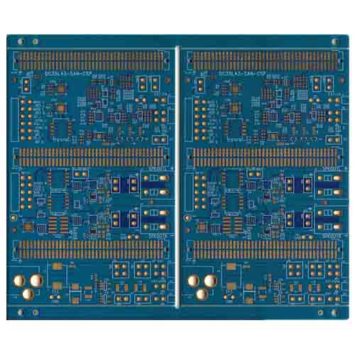
Twelve-layer second-order board
name: Twelve-layer second-order board
Plate: FR4
Layers: 12L
Material: ISOLA
Plate Thickness: 2.0mm
Copper thickness of inner and outer layers: 1oz
Minimum hole diameter: 0.1mm
Surface Treatment: Immersion Gold
Line width: 0.1mm
Line distance: 0.1mm
BGA pad: 0.15mm
Special craftsmanship: second stage
Use: consumer electronics
Standard for good 12-layer pcb stackup
A. Ground planes are preferred because of their ability to route signals in a microstrip configuration.
B Ground plane based 12-layer PCB with low ground impedance and low noise.
C. The middle layer between layers is used as the trace for high-speed signals. Even in adjacent planes, the signal layers must be tightly packed with each other.
D. You must place the plane and signal layers in adjacent layers.
E. The large plan and power planes are tightly coupled together.
When choosing a 12-layer stack, our expert design team focused on the following:
The signal layer should always be adjacent to the plane
The power plane can be used for the return path of the signal
Signal layers should be tightly coupled to their adjacent planes
Determine the return portion of the signal
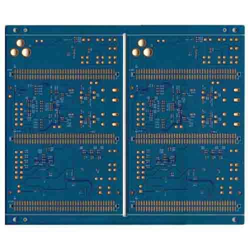
name: Twelve-layer second-order board
Plate: FR4
Layers: 12L
Material: ISOLA
Plate Thickness: 2.0mm
Copper thickness of inner and outer layers: 1oz
Minimum hole diameter: 0.1mm
Surface Treatment: Immersion Gold
Line width: 0.1mm
Line distance: 0.1mm
BGA pad: 0.15mm
Special craftsmanship: second stage
Use: consumer electronics
- Previous:No
- Next:Communication equipment 2-stage HDI PCB board
