

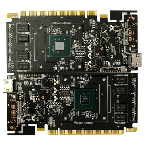
computer graphics card BGA assembly
Name: computer graphics card BGA assembly
Number of SMT lines: 5 high-speed SMT patch supporting production lines
SMT daily production capacity: more than 15 million points
Testing Equipment: X-RAY Tester, First Piece Tester, AOI Automatic Optical Tester, ICT Tester, BGA Rework Station
Placement speed: CHIP component placement speed (at best conditions) 0.036 S/piece
The smallest package that can be attached: 0201, the accuracy can reach ±0.04mm
Minimum device accuracy: PLCC, QFP, BGA, CSP and other devices can be mounted, with a pin pitch of ±0.04mm
IC type patch accuracy: It has a high level for mounting ultra-thin PCB boards, flexible PCB boards, gold fingers, etc. It can be mounted/inserted/mixed with FTT display driver boards, mobile phone motherboards, battery protection circuits and other difficult products
With the advancement of integration technology, improvement of equipment, and the use of deep submicron technology, LSI, VLSI, and ULSI have appeared one after another, the integration level of silicon single chips has continued to increase, the requirements for integrated circuit packaging have become more stringent, and the number of I/O pins has increased sharply , power consumption also increases. In order to meet the needs of development, on the basis of the original packaging varieties, a new variety has been added - ball grid array packaging, referred to as BGA
The long needle-like pins are changed to contacts, and the contacts are placed on the bottom of the chip, and connected to the PCB through ball solder. This is our common BGA ball matrix array package.
The BGA package has the following characteristics: 1. The number of input and output pins is greatly increased, and the pin spacing is much larger than that of QFP, plus it has an automatic alignment function with circuit graphics, thereby improving the assembly yield; 2. Although its power The power consumption increases, but it can be welded by the controlled collapse chip method, and its electrothermal performance has been improved. For chips with high integration and high power consumption, a ceramic substrate is used, and a miniature exhaust fan is installed on the shell to dissipate heat. To achieve stable and reliable operation of the circuit; 3. The thickness of the package body is reduced by more than 1/2 compared with ordinary QFP, and the weight is reduced by more than 3/4; 4. The parasitic parameters are reduced, the signal transmission delay is small, and the frequency of use is greatly improved; 5. The assembly can be shared Surface welding, high reliability.
However, the BGA package is not perfect. Like QFP and PGA, the BGA package still occupies too much substrate area; the warping problem of the plastic BGA package is its main defect, that is, the coplanarity of the solder balls. The standard of coplanarity is to reduce warpage and improve the characteristics of BGA packaging. Plastics, die attach adhesives and substrate materials should be studied and optimized. At the same time, due to the high cost of the substrate, the price is high.
In the graphic accelerator chip industry, BGA packaging has been used since the classic nVIDIA Riva 128 and ATi Rage Pro in 1998. Since then, BGA packaging has become the only choice for graphics accelerator chips. It was not until Geforce FX series products that they began to use BGA packaging. FC-BGA packaging method.
As the heat generated by the 3D graphics accelerator chip gradually increases, the heat dissipation problem of BGA becomes more and more serious. At this time, many manufacturers have improved the BGA package for this point, and installed a metal top for auxiliary heat dissipation on the top of the BGA package. Cover, thereby prolonging the life cycle of the BGA package, which is the Wirebond package.
BGA package is a surface mount package chip used for an integrated circuit. In fact, it is an auxiliary equipment used in BGA soldering technology. The grid is the grid, which is used to position the BGA pins on the PCB pad; the ball is the solder ball, or solder paste, and the solder ball is placed on the solder pad. On the plate, it is called planting balls. The pins are ball-shaped and arranged in a grid-like pattern, hence the name BGA.
When it comes to BGA packaging, we must talk about its advantages:
1. Small size and large memory, the same memory product with the same capacity, the volume is only one-third of the TSOP package.
2. The pins of the previous package form are distributed around. When there are many pins, the spacing is reduced to a certain extent, and the pins are easy to deform. However, the BGA solder balls are at the bottom of the package, and the spacing increases instead, which greatly improves the yield.
3. Good electrical performance. The BGA pins are very short, and solder balls are used instead of leads, which makes the signal path short, reduces lead inductance and capacitance, and enhances electrical performance.
4. Good heat dissipation. The contact surface between the spherical contact array and the substrate is large and short, which is good for heat dissipation.
5. Good coplanarity, high reliability!
he emergence of BGA packaging has become the best choice for high-density, high-performance, multi-pin packaging such as CPUs and south/north bridge chips on motherboards.

Name: computer graphics card BGA assembly
Number of SMT lines: 5 high-speed SMT patch supporting production lines
SMT daily production capacity: more than 15 million points
Testing Equipment: X-RAY Tester, First Piece Tester, AOI Automatic Optical Tester, ICT Tester, BGA Rework Station
Placement speed: CHIP component placement speed (at best conditions) 0.036 S/piece
The smallest package that can be attached: 0201, the accuracy can reach ±0.04mm
Minimum device accuracy: PLCC, QFP, BGA, CSP and other devices can be mounted, with a pin pitch of ±0.04mm
IC type patch accuracy: It has a high level for mounting ultra-thin PCB boards, flexible PCB boards, gold fingers, etc. It can be mounted/inserted/mixed with FTT display driver boards, mobile phone motherboards, battery protection circuits and other difficult products
- Previous:No
- Next:High-end projector motherboard BGA assembly
