

Camera Module Rigid-Flex PCB Assembly
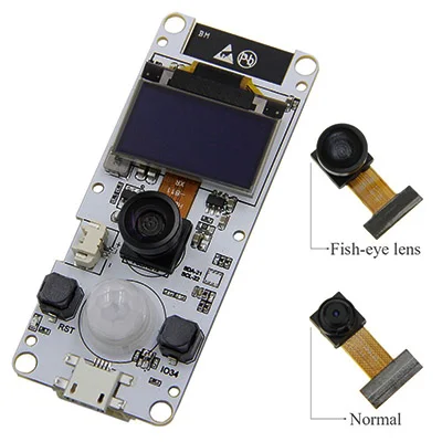
Name: FPC OV2640 Camera Module PCB Assembly
BGA mounting range: 0.18mm-0.4mm
Minimum placement material package: 01005
Minimum line width/spacing: 3mil/3mil
BGA pitch: 0.25mm
Minimum diameter of finished product: 0.1mm
Maximum size: 610mmX1200mm
Thickness: 0.3-3.5mm
Production equipment: 1 MYDATA solder paste jet printer, 1 solder paste detector, 2 MYDATA placement machines, 3 YAMAHA placement machines, 3 reflow soldering machines, and 1 wave soldering machine
With the continuous expansion of communication technology, mobile phones have become an indispensable tool for people's life, work, study and entertainment. The mobile phone camera module is one of the very important components in the mobile phone, and its quality directly affects the overall quality of the mobile phone. Therefore, every step in the production process of mobile phone camera modules must be strictly checked, and there should be no slack in the slightest. In the mobile phone camera module, the FPC flexible circuit board is one of the key components that determine the pictures generated by the mobile phone camera, so its production process and quality are particularly important.
Based on this, the principle of the mobile phone camera module and the application of SMT technology in the production process of the mobile phone camera module are briefly introduced first, and the improved design of the FPC flexible circuit board of the mobile phone camera module and the SMT production process and product quality analysis are emphatically explained. According to the specific requirements of the FPC flexible circuit board of the mobile phone camera module, the SMT technical index is optimized reasonably, and the SMT welding temperature distribution curve of the mobile phone camera module reflow soldering is analyzed and studied. AIO (automatic optical inspection) detection and ICT online testing methods are set up for FPC soft circuit board products.
1.1 Introduction to Mobile Phone Camera Module
1.1.1 Principle
The mobile phone camera module is mainly composed of four parts: lens (lens), sensor (sensor), image processing chip (Backend IC), and flexible circuit board (FPC). Its working principle is: the scene is shot through the lens, the optical image is generated and projected onto the sensor, and then the optical image is converted into an electrical signal, and the analog electrical signal is converted into a digital signal through analog-to-digital conversion, processed by DSP, and sent to the mobile phone for processing After processing in the device, it is converted into an image that can be seen on the screen of the mobile phone
1.1.2 DSP chip
DSP is a digital signal processing integrated circuit. Its function is to optimize the digital image signal through mathematical algorithm operation, and the processed signal is transmitted to the display device. At present, DSP design and production technology are relatively mature, and there is little difference in various technical parameters. The chips of the mobile phone camera module mainly include CCD and CMOS. The chip of the mobile phone camera module is shown in Figure 1-2, and the performance comparison is shown in Table 1-1. According to the performance comparison between CCD and CMOS chips, CMOS chips have the advantages of relatively simple manufacturing process, high qualified rate of finished products, low manufacturing cost, low power consumption, and fast processing speed. CMOS chips.
1.1.3 Connection method
The common connection methods of mobile phone camera modules include connector connection, golden finger connection and socket connection. In this paper, the mobile phone camera module adopts the gold finger connection method, which is suitable for the cooperation with the mobile phone, with good bending degree and high reliability.
1.1.4 PCB board
PCB boards are usually divided into three types: rigid boards, flexible boards, and rigid-flex boards. This refers to the printed circuit boards used in mobile phone camera modules. These three materials have different application ranges. CMOS can use any kind of hard board, soft board, and soft-rigid board. Rigid-flex boards have the highest cost, while CCDs can only use rigid-flex boards. Therefore, the mobile phone camera module in this article uses FPC soft circuit board,
1.2 Application of SMT technology in the production process of mobile phone camera modules
1.2.1 Functions of FPC flexible circuit board (PCB)
The FPC flexible circuit board has the following functions in the mobile phone camera module: to provide mechanical support for the fixing and assembly of electronic components, to realize the wiring between electronic components and to have a connection or electrical insulation effect on electricity, and to provide the required electrical components. characteristic. Provides solder resist maps for automatic soldering, and provides identification graphics and characters for integrated circuit and component insertion, inspection, and maintenance. After the mobile phone camera module adopts PCB, due to the consistency of similar PCB boards, manual wiring errors are avoided, and automatic insertion, automatic placement, automatic soldering and automatic detection of integrated circuits and electronic components can be realized, making electronic products more reliable. Quality and labor productivity are improved, while costs are reduced and maintenance is facilitated.
1.2.2 Application of SMT technology
At present, mobile phone camera modules have the characteristics of small size, light weight, high integration, and high reliability. The main form of electronic products is board-level electronic circuit products of substrates. Therefore, an important embodiment of modern electronic product manufacturing technology is board-level The level of manufacturing technology of electronic circuit products. The mobile phone camera module belongs to the chip level package. First, the silicon chip (chip) is mounted on the substrate, and then welded to the substrate to form a complete component. The core technology of the SMT product manufacturing system is SMT surface assembly technology, a system that takes SMT products as the manufacturing object, and the production line composed of surface assembly equipment is the basic form of SMT. The surface assembly equipment is connected by automatic transmission lines, and the configuration computer is used as the control system. , control the automatic transmission of PCB, and carry out assembly work through assembly equipment.
Improved design of mobile phone camera module
2.1 FPC/PCB layout design
For electronic products, the rationality of its design is closely related to product production and product quality. The layout of the FPC printed wires of the mobile phone camera module should be as short as possible, and the wiring distance between the patch and the state line should be greater than 0.3 mm, to prevent the solder paste from reflowing to the Bangxian PAD during SMT placement.
The inner edge of Bangxian PAD is between 0.1mm and 0.35mm from the chip, the outer edge of Bangxian PAD is more than 0.1mm away from the Holder, the distance between the capacitor and the inner wall of the Holder must be more than 0.1mm, and the capacitor must be close to the chip filter PAD.
The FPC connected by the gold finger needs to open the window of the entire gold finger. For the double-sided gold finger, the top layer and the bottom layer must be staggered to open the window, and the staggered distance must be more than 0.25mm.
The window shape of the FPC silver foil grounding is elliptical, and the positions of the double-sided windows must be staggered, no overlapping parts are allowed, and the stagger distance is guaranteed to be more than 0.5mm.
2.2 FPC/PCB circuit design
In order to enable the camera module to work normally, the width of the wire should meet the electrical performance requirements. It is convenient for production and can effectively prevent EMC, EMI and other problems. Magnetic beads, inductors, and common mode coils can be used for isolation; capacitors are added for filtering, and copper is laid everywhere, and shielding ground wires and shielding planes are used to cut off electromagnetic conduction and radiation pathways. The following are the requirements and specifications for module circuit design:
(1) The distance between the network and the edge of the outer frame is greater than 0.15mm, that is, greater than the outer frame tolerance +0.1mm.
(2) The recommended line width of general signal lines is 0.1mm, and the minimum line width is 0.08mm; the recommended line width of power lines and ground lines is 0.2mm, and the minimum line width is 0.15mm.
(3) Avoid circular lines, and no right angles are allowed on the lines.
(4) Holes are drilled in the blank area of the line, which plays the role of shielding and heat dissipation, and at the same time increases the connectivity between DGND networks. For FPC, if there are bending requirements in the controlled project drawings, in the bending area of FPC, use ground wire instead of copper laying to avoid poor bending of FPC caused by large-scale copper laying.
(5) AGND follows the signal line, and try not to have a DATA line nearby.
(6) MCLK should cover the ground, the wiring distance should be as short as possible, and via holes should be avoided as much as possible. Do not go together with high-speed data bits for PCLK, cover the ground as much as possible, have DGND next to it, and D0 and PCLK are close to DGND.
(7) Reset RESET and STANDBY should be far away from MCLK, close to DGND, and shielded with ground near the edge.
(8) It is not allowed to drill holes on the PAD on the bottom of the Socket. If it is unavoidable, the holes should be drilled on the edge of the PAD, more than 0.4mm away from the connection point, and must be filled with metal to ensure that the entire surface that contacts the PAD is covered. is conductive.
(9) The MIPI differential impedance line pair needs to meet the requirement of an impedance value of 100±10ohm, and the MIPI traces must be of equal length, equal spacing, and have a larger reference ground plane.
2.3 FPC/PCB process material
For high-frequency circuits, the material of the PCB is very important. Commonly used PCB boards include bakelite boards, paper resin boards, and glass resin boards. The mobile phone camera module is made of glass resin board, the highest frequency is 1GHZ, the price is medium, and the texture is hard. It is the most widely used variety at present.
(1) There are two options for FPC process materials
COB project head ACF pressure welding: the surface treatment method is chemical gold, the base material is 18um glue-free rolled copper, Au≥0.03um, Ni≥0.5um gold surface is smooth and bright; CSP project head patch: the surface treatment method is chemical gold , the substrate is optional (18um non-adhesive rolled copper, 18um glued rolled copper, 13um electrolytic copper), Au≥0.03um, Ni≥2.54um gold surface is smooth and bright.
COF process: the surface treatment method is nickel-palladium-gold, and the base material is optional (13um, 18um without glue and glued rolled copper, 13um, 18um without glue and glued electrolytic copper), 8um≥nickel thickness≥4um, 0.15um≥ Palladium thickness ≥ 0.08um, 0.15um ≥ gold thickness ≥ 0.08um.
(2) Electromagnetic membrane model: In addition to the model specified by the customer, PC5600 or PC5900 with better flexibility should be selected. (3) Lamination structure: The lamination structure confirmed with the FPC supplier needs to meet the FPC thickness required by the customer. After the customer confirms, the lamination material cannot be changed without authorization. If the material is to be changed, the customer's approval is required.
2.4 Module Packaging Design
(1) According to the project-controlled drawings, pre-design pallets, sponge pads, adhesive paper, etc.
(2) Sponge pads and adhesive tape must be used on a completely OK module for actual measurement, and compared with the requirements of the project's controlled drawings. If there is a difference, according to the actual situation of the module, make a new sample until the requirements are met.
(3) The tray must be tested with the final molded module (such as sticking sponge pads, tapes, sponge rings, dust-proof stickers, etc. on the module as required), and the entire module must not be squeezed; and the tray must It has relative hardness to ensure that the extrusion between the pallets in the whole box does not affect the internal modules.
3. SMT production process of mobile phone camera module FPC flexible circuit board
The SMT production process of mobile phone camera module is as follows:
Incoming material inspection --> PCB surface silk screen solder paste --> patch --> drying (curing) --> reflow soldering --> inspection --> repair
3.1 Incoming inspection
In the production process, the PCB and electronic components of the mobile phone camera module FPC flexible circuit board must undergo quality inspection before entering the production line. This process is called IQC (Incoming Quality Control). First, visually inspect the PCB of the FPC flexible circuit board, and then inspect the substrate through the inspection instrument, mainly checking the thickness and plug-in pinholes. The components of the FPC flexible circuit board include parameter inspection of resistors and capacitors, open circuit, short circuit, etc. . PCB and components enter the next process after passing the incoming quality control inspection. The pre-processing test provides the primary guarantee for the entire production process of the mobile phone camera module FPC flexible circuit board, and at the same time improves the pass rate of the product.
3.2 Solder paste printing
Before patching, a solder paste printing machine must be used to scrape solder paste on the pinholes and welding parts of the FPC flexible circuit board of the mobile phone camera module. On the operating table of the solder paste printing machine, use a monitor to observe, use a stencil to align the pinholes and soldering parts of the PCB board, and pay attention to ensure accurate positioning. Then the solder paste printing machine can apply the solder paste evenly and without deviation on the PCB board through the corresponding position of the stencil, so that it is ready for the welding of components, and finally sent to the SMT production line
3.2.1 Main technical indicators
The PCB board area of the mobile phone camera module is small, which is different from other large circuit boards, and the precision requirements are very high, so this indicator should be considered in printing.
a. Maximum printing area: determined as 120mmх120mm according to the largest PCB size.
b. Printing accuracy: ±0.025mm is required.
c. Printing speed: determined according to output requirements.
3.2.2 The principle of printing solder paste
Both solder paste and adhesive are viscous, thixotropic fluids. When the scraper moves at a certain speed and angle, it will exert a certain pressure on the solder paste, so that the solder paste will roll in front of the scraper, and the solder paste will be injected into the mesh or leak hole, and the viscous friction of the solder paste will cause the solder paste to Shear occurs at the junction of the scraper and the stencil, and due to the shear force, the viscosity of the solder paste decreases, and the solder paste is smoothly injected into the mesh or leak hole of the PCB board in the mobile phone camera module.
3.2.3 Solder paste inspection
Use the 3D solder paste inspection machine to test the thickness of the solder paste printed on the PCB board of the mobile phone camera module, mainly to detect the "height", "area" and "volume" of the solder paste. Of course, the "height" detection is the most important. One of the important indicators to measure the quality and reliability of solder joints is the amount of solder paste, especially for mobile phone camera modules. In order to reduce solder joint defects in the printing process, 100% solder paste inspection (SPI ), which also ensures the reliability of the solder joints.
3.3.1 Mounter
The PCB board placement of the mobile phone camera module is completed through the placement machine. Before the placement, the raw material tray is first installed in front of the placement machine, and the patch type components are installed on the raw material tray transmission tape of the raw material box. The operation process is completed through the pre-programmed program of the single-chip computer, and the laser system is calibrated. During placement, the placement machine operates according to the pre-set program. The components on the corresponding raw material tray are sucked by the suction nozzle of the mechanical arm and placed on the corresponding position of the PCB board. In order to ensure that the components can be accurately pressed on the corresponding welding position , using a laser to correct the components.
Multiple raw material trays can be placed on the same high-speed placement machine to work at the same time. The size of the components is required to be similar, so that the robotic arm is easy to operate. In order to improve efficiency, the SMT production line of mobile phone camera modules is completed by two high-speed placement machines. The component suction nozzles of the placement machines should be the same according to the size of the components. Resistor"), and then mount larger chips (such as "chipsets").
3.3.2 Main technical indicators of placement machines
Combined with the specific performance requirements of the flexible circuit board of the mobile phone camera module, the main indicators of the placement machine are reasonably set:
a. Mounting accuracy: refers to the offset of the standard mounting position of the printed board after the component is mounted. The PCB mounting accuracy of the mobile phone camera module is higher, and the Chip component is required to reach ±0.1mm. The SMD requires at least ±0.06mm.
b. Mounting speed: The PCB area of the mobile phone camera module is small, so the mounting speed should not be too fast. The high-speed machine is limited to below 0.2S/Chip component, and the multi-function machine is set around 0.3-0.6S/Chip component.
c. Alignment method: In order to ensure accuracy, try to use laser alignment or laser/vision hybrid alignment.
d. Placement function: refers to the ability to place components. The multi-function machine mounts devices with a minimum size of 0.6×0.3mm and a maximum size of 60×60mm.
e. Programming function: It has online and offline programming optimization functions.
3.3.3 Problems that should be paid attention to in continuous placement production
Since the flexible circuit board of the mobile phone camera module has special requirements, there are strict requirements in the component placement process:
a. It is forbidden to directly touch the surface of the PCB with hands to prevent damage to the printed solder paste;
b. When an alarm is found, press the alarm off button in time to analyze and process the error message;
c. According to the type, specification, polarity and direction of components, they must be consistent when supplementing components;
d., Pay attention to the discarded materials in the waste tank during the placement process at any time. If the accumulation is too high, it should be cleaned in time to prevent the placement head from being damaged.
3.4 Reflow selling ring
The reflow oven is a device for soldering surface mount components. Infrared heating stoves and full hot blast stoves are widely used. The reflow furnace mainly has four parts: infrared furnace, hot air furnace, infrared heating furnace, steam welding furnace.
After the FPC components of the mobile phone camera module are installed, qualified products are welded by a reflow soldering machine. The reflow welding machine is an internal circulation heating system consisting of multiple temperature zones. Because solder paste is composed of many materials, different temperatures will change the state of the solder paste. The solder paste becomes liquid in the high temperature zone, and the chip components are easy to combine. The solder paste becomes solid after entering the colder temperature zone, and the component pins and the PCB are firmly welded together.
3.4.1 Basic structure of reflow oven
a. Furnace body
b. Up and down heating source
c. Temperature control device
d. Cooling device
e. Air circulation device
f. Exhaust device
g.PCB transmission device
h. Computer control system
3.4.2 Main technical indicators of reflow oven
Combined with the specific performance requirements of the flexible circuit board of the mobile phone camera module, the main indicators of the placement machine are reasonably set:
a. Transverse temperature difference of the conveyor belt: ±5°C or less;
b. Temperature control accuracy: should reach ±0.1-0.2°C;
c. The mobile phone camera module does not use lead-free solder or metal substrate, and the temperature is selected at about 250°C.
d. Select 4-5 temperature zones according to the number and length of the heating zone of the mobile phone camera module, and the length of the heating zone is selected to be about 1.8m.
3.4.3 Analysis of reflow soldering process
In order to analyze and study the mobile phone camera module, a temperature curve collector was purchased to conduct temperature curve testing. Analysis of the temperature curve collected by the temperature curve collector: When the soft board of the mobile phone camera module enters the heating zone (dry zone), that is, below 100oC, the solvent and gas in the solder paste evaporate, and at the same time, the solder pads and component terminals The pins and pins are wetted by the flux in the solder paste, the solder paste softens, collapses, covers the pad, and isolates the pad, device pins and oxygen. The time is about 15S; when the PCB enters the heat preservation zone, the temperature is 100oC-150oC, the PCB and components are fully preheated, the time is about 30S, and the PCB and components are prevented from being damaged when the heat preservation zone transitions to the high temperature zone; when the PCB enters the welding zone, the temperature rises rapidly to above 240oC, making the solder paste Melting into a liquid state, the pads, component terminals and pins of the PCB are wetted by the liquid solder, and diffuse, flow or reflow to form a solder; after that, the PCB enters the cooling zone to solidify the solder joints.
3.4.4 Process characteristics of reflow soldering (compared with wave soldering technology)
In the production of mobile phone camera modules, the reflow soldering assembly process is used instead of wave soldering technology. Reasons:
a. Reflow soldering is not like wave soldering, it does not need to immerse components directly in molten solder, it has a large thermal stress, and the thermal shock to the components is small;
b. The amount of solder applied on the pad can be properly controlled, avoiding the occurrence of welding defects such as virtual solder bridging, and improving the welding quality and reliability;
c. When using solder paste, the composition of the solder can be ensured correctly, and impurities will not be mixed into the solder.
d.Self alignment—Due to the surface tension of molten solder, when the component placement position is offset, it is automatically pulled back to the approximate target position.
e. On the same substrate, local heating heat sources and different welding processes can be used for welding;
f. The process is simple, and the workload of panel repair is extremely small, thus saving manpower, electricity and materials.
SMT application analysis of mobile phone camera module FPC flexible circuit board
4.1 Inspection of welding and assembly quality
After reflow soldering, the final process is to inspect the soldering quality and assembly quality of the PCB board of the assembled mobile phone camera module. The equipment used includes magnifying glass, microscope, automatic optical inspection (AOI), online tester (ICT), etc. On the special inspection table, use a plastic template to compare with the patch PCB to check whether the position on the PCB is correct, whether the pins are soldered, whether the components are missing soldered, whether the soldering is tight, etc. Quality inspectors should wear electrostatic wristbands to prevent damage caused by static electricity during the inspection process. PCBs that fail the quality inspection will be sent to the maintenance department of the SMT production line, and the solder joints, positions and missing solder components will be manually corrected, and then returned to the inspection after correction.
4.1.1 Automatic optical inspection
Using high-speed and high-precision visual processing technology to automatically detect various mounting errors and welding defects on the PCB board of the mobile phone camera module. The range of PCB boards can range from high-density boards to low-density large-size boards. In order to improve production efficiency and welding quality, an online inspection solution is adopted.
Tools to Reduce Defects Using AOI inspection machines, good process control can be achieved because errors can be found and eliminated early in the assembly process. Early detection of defects can effectively avoid sending bad boards to the assembly stage, and AOI not only reduces repair costs, but also avoids scrapping unrepairable boards.
Defects in the manufacturing process and bad conditions of components, such as missing parts, displacement and component skew, tombstones, flipped parts, floating feet and bent leads, etc., can be found directly by testing the electrical performance of online devices.
In addition, the characteristics of AOI are also obvious. The high-speed detection system has nothing to do with the patch density of the PCB board. It can be programmed quickly and conveniently under the graphical interface, automatically detects with the placement data, and quickly edits the detection data with the component database. The detection window is automatically corrected according to the instantaneous change of the position of the detected component to achieve high-precision detection. Detection and verification is done by marking with ink directly on the PCB board or by graphical error representation on the operator display.
4.1.2 AOI detection steps
Mobile phone camera module products are tested according to the following steps:
a. Put the PCB board into the AOI machine according to the correct flow direction.
b. After the AOI test is completed, the operator removes the board from the conveyor belt with both hands, and uses the Barcode Reader to read the serial number.
c. Confirm that the direction of the PCB is consistent with the Layout display, the relevant position and its defect are displayed on the screen, and the operator confirms according to the defect position.
d. After the test is confirmed as Pass, you need to flash the SFC system and send it directly to the next process. If it is confirmed as Fail, flash the SFC system, enter the defective code, put it into the defective product box, and repair it by online personnel. After the repair is OK, put it into the AOI Machine test, until the test is OK before sending to the next process.
4.2 ICT online test
4.2.1 Overview
ICT is a test method to check manufacturing defects and defective components by testing the electrical properties and electrical connections of online components. It mainly checks the open circuit and short circuit of individual components on-line and each circuit network. It has the advantages of simple operation, fast and accurate fault location, etc.
1. Scope and characteristics of ICT
The online test checks the electrical performance of the online components on the manufactured board and the connection of the circuit network. Not only can quantitatively measure resistance, capacitance, inductance, crystal oscillator and other components, but also can test functions such as diodes, triodes, optocouplers, relays, operational amplifiers, transformers, power modules, etc. , Memory, exchange and other ICs for functional testing.
Components can check out the failure or damage of component values, out-of-tolerance, program errors in Memory, etc., and find defects in manufacturing processes and defective components by directly testing the electrical performance of online devices. For the process category, faults such as solder short circuit, wrong component insertion, reverse insertion, missing installation, lifted pins, virtual soldering, PCB short circuit, and disconnection can be found.
The maintenance of faults does not require much professional knowledge, and the faults tested are directly located on specific component pins and network points, and the fault location is accurate.
2. Meaning
The faulty board tested by ICT can greatly improve production efficiency and reduce maintenance cost because of accurate fault location and convenient maintenance. Online testing is usually the first testing process in production, which can reflect the production status in a timely manner and is conducive to process improvement and upgrading. Because of its specific test items, it is one of the important test methods for modern mass production quality assurance.
4.2.2 ICT online test steps
According to the requirements of mobile phone camera module products, reasonably arrange the ICT online test steps:
a. Remove the board from the line with both hands, put it flat on the jig, pay attention to the direction of the board, and confirm that the board is flat on the jig.
b. Press and hold the test button with both hands at the same time to test, and let go after the test starts.
c. If the test result is pass, mark "Pass" in the position area of the picture on the edge of the board, enter the next process on the assembly line, and place the board in the same direction.
d. If the test result is fail, print the bad report and paste it on the edge of the board, and put it in the defective product box to be confirmed by the line repair: if it is a misjudgment, notify the ICT engineer to analyze and process and retest the ICT until Pass; if it is bad, repair the line Send it to the ATE station to flash the bad information into the sfc system, then repair and retest the ICT until the test passes, and flow into the next process.
We provide Camera Module Rigid-Flex PCB Assembly Rigid-Flex PCB Assembly services. Kingford is your one-stop rigid-flex circuit board assembly company.、

Name: FPC OV2640 Camera Module PCB Assembly
BGA mounting range: 0.18mm-0.4mm
Minimum placement material package: 01005
Minimum line width/spacing: 3mil/3mil
BGA pitch: 0.25mm
Minimum diameter of finished product: 0.1mm
Maximum size: 610mmX1200mm
Thickness: 0.3-3.5mm
Production equipment: 1 MYDATA solder paste jet printer, 1 solder paste detector, 2 MYDATA placement machines, 3 YAMAHA placement machines, 3 reflow soldering machines, and 1 wave soldering machine
- Previous:Medical Device Rigid-Flex PCB Assembly
- Next:FPC PCB Assembly
