

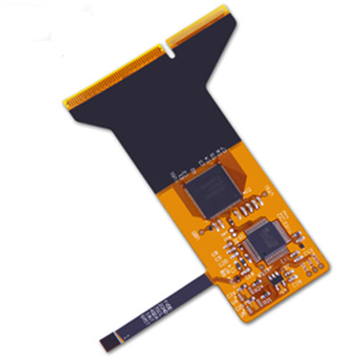
4-layer flexible PCBs
Name: 4-layer flexible PCBs
BGA mounting range: 0.18mm-0.4mm
Minimum placement material package: 01005
Minimum line width/spacing: 3mil/3mil
BGA pitch: 0.25mm
Minimum diameter of finished product: 0.1mm
Maximum size: 610mmX1200mm
Thickness: 0.3-3.5mm
Production equipment: 1 MYDATA solder paste jet printer, 1 solder paste detector, 2 MYDATA placement machines, 3 YAMAHA placement machines, 3 reflow soldering machines, and 1 wave soldering machine
First, the advantages of flexible PCB
1. Flexibility
A significant advantage of using a flexible PCB is that it can be more conveniently routed and connected in three-dimensional space, and can also be rolled or folded for use. As long as it is curled within the allowable radius of curvature, it can withstand thousands to tens of thousands of uses without damage.
2. Reduce the volume
In the assembly and connection of components, compared with the use of wires and cables, the conductor cross-section of the flexible PCB is thin and flat, which reduces the size of the wires and can be shaped along the casing, making the structure of the device more compact and reasonable, reducing the need for assembly and connection. volume. Compared with rigid PCB, the space can be saved by 60~90%.
3. Reduce weight
In the same volume, compared with the wire and cable, the weight of the flexible PCB can be reduced by about 70% under the same current carrying capacity, and compared with the rigid PCB, the weight can be reduced by about 90%.
4. Consistency of installation
It is installed and connected with flexible PCB, which eliminates the errors when wiring with wires and cables. As long as the processing drawings are verified and passed, all the winding circuits produced later will be the same. There will be no misconnection when installing the connecting wire.
5. Increased reliability
Kingford is a one-stop solution provider for professional 4-layer flexible PCBs, flexible PCB assembly.
4-layer PCBs are commonly used in various applications, these PCBs are a key part of various electronic devices as well as communication equipment. Would you like to know more about them, especially stack structures and their types? What benefits do they provide and what are their areas of application? Read through the post and you will get all your questions answered.
What is a four-layer PCB?
Of all the multilayer types, the most common is the 4-layer printed circuit board (PCB). The stackup of 4-layer PCB is very strong, it consists of top layer, inner layer 1, inner layer 2 and bottom layer for routing electrical signals. Both inner layers (inner layers 1 and 2) are located between the top and bottom layers. Therefore, a four-layer PCB means 2 signal layers + a positive voltage layer (VCC layer) + a ground layer (GND layer) or 3 signal layers + GND layer. In a 4-layer PCB design, more surface area is available for traces. Therefore, this design structure provides excellent routing for both low-speed and high-speed signals.
Four-layer PCB stack-up type
When you contact Kingford manufacturer, they will provide you with these two standard constructions for a 4-layer PCB. The VCC and GND layers here are organized according to the application requirements.
Type 1: Signal – GND – VCC – Signal: In this 4-layer PCB design, the top layer is preferably the critical signal. In terms of layer thickness, the impedance control core board should not be too thick. This helps reduce the distributed impedance of the ground plane and power supply.
Type 2: GND - Signal - Signal - GND: This stackup is ideal if you don't want to use via paths to connect all types of ground pins. To improve the EMC performance of the board, it is a good idea to always place signal layers close to the planes. Utilize large cores between the ground and power planes to maintain the overall thickness of the substrate.
The main advantages of four-layer PCB
Due to its beneficial properties, four-layer PCBs are widely used in many electronic applications. Some of the key advantages offered by these multilayer PCBs are as follows:
1. Smaller mass-driven design: This is one of the important reasons for using 4-layer PCBs. Due to their multi-layer design, they are inherently smaller than single-sided PCBs. This is beneficial for modern electronic devices such as smartphones, tablets and laptops. Since it is a multi-layer design, it requires a thoroughly planned design and precision when installing components. This helps reduce unnecessary errors and ensures high-quality results.
2. Excellent durability: As mentioned above, these circuit boards can not only bear the weight, but also withstand the pressure and heat applied, so that they are bonded together. Plus, their durability is increased due to the multi-layer insulation between circuit layers.
3. Higher packing density: These printed circuit boards increase packing density by combining multiple layers onto one board. The interconnection between the proximal regions makes the connection between the boards closer.
4. Lightweight structure: In a 4-layer PCB, multiple connectors are required to interconnect or connect separate single-layer and double-layer circuit boards. It helps to simplify circuit design and reduce its weight.
Application of four-layer PCB
The key advantages of these boards contribute to their popularity in various industries. Following are some important applications where these boards are widely used:
For example: heart monitors, computers, GPS technology, file servers, mobile phones, data storage, signal transmission, weather analysis, space probe equipment, X-ray equipment, atomic accelerators, cat scanning technology, fiber optic receivers, central fire alarm systems, Cell Phone Transmitters and Repeaters.
Kingford is a one-stop solution provider for professional 4-layer flexible PCBs, flexible PCB assembly.

Name: 4-layer flexible PCBs
BGA mounting range: 0.18mm-0.4mm
Minimum placement material package: 01005
Minimum line width/spacing: 3mil/3mil
BGA pitch: 0.25mm
Minimum diameter of finished product: 0.1mm
Maximum size: 610mmX1200mm
Thickness: 0.3-3.5mm
Production equipment: 1 MYDATA solder paste jet printer, 1 solder paste detector, 2 MYDATA placement machines, 3 YAMAHA placement machines, 3 reflow soldering machines, and 1 wave soldering machine
