

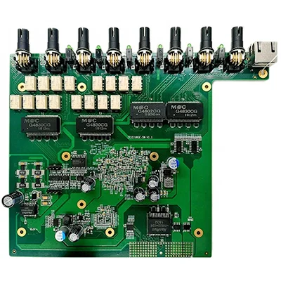
GPS Tracker Circuit PCBA Board
Name: GPS Tracker Circuit PCBA Board
The number of layers that can be copied: 1-32 layers
Minimum line width and line spacing: 3mil
Minimum laser aperture: 4mil
Minimum mechanical aperture: 8mil
Copper foil thickness: 18-175цm (standard: 18цm35цm70цm)
Peel strength: 1.25N/mm
Minimum punching hole diameter: single side: 0.9mm/35mil
Minimum hole diameter: 0.25mm/10mil
Aperture tolerance: ≤φ0.8mm±0.05mm
Hole tolerance: ±0.05mm
Hole wall copper thickness: double-sided/multi-layer: ≥2um/0.8mil
Hole resistance: double-sided/multi-layer: ≤300цΩ
Minimum line width: 0.127mm/5mil
Minimum pitch: 0.127mm/5mil
Surface treatment: rosin spray tin electric gold, anti-oxidation, chemical gold, carbon oil
Warpage: ≤0.7%
The Global Positioning System (GPS) is a high-precision radio navigation positioning system based on artificial earth satellites. It can provide accurate geographic location, vehicle speed and Precise time information. Since its inception, GPS has attracted many users with its high precision, all-weather, global coverage, convenience and flexibility. GPS is not only the patron saint of automobiles, but also the wisdom of logistics industry management. With the rapid development of the logistics industry, GPS has played a pivotal role and has become the second largest consumer group after the automobile market.
GPS PCB antennas come in two forms: active and passive. Active antennas have a low noise amplifier (LNA) built into the module, while passive antennas do not include an amplifier. Active antennas are on their own board and are connected to your printed circuit board via coaxial cables.
Name: GPS Tracker Circuit PCBA Board
The number of layers that can be copied: 1-32 layers
Minimum line width and line spacing: 3mil
Minimum laser aperture: 4mil
Minimum mechanical aperture: 8mil
Copper foil thickness: 18-175цm (standard: 18цm35цm70цm)
Peel strength: 1.25N/mm
Minimum punching hole diameter: single side: 0.9mm/35mil
Minimum hole diameter: 0.25mm/10mil
Aperture tolerance: ≤φ0.8mm±0.05mm
Hole tolerance: ±0.05mm
Hole wall copper thickness: double-sided/multi-layer: ≥2um/0.8mil
Hole resistance: double-sided/multi-layer: ≤300цΩ
Minimum line width: 0.127mm/5mil
Minimum pitch: 0.127mm/5mil
Surface treatment: rosin spray tin electric gold, anti-oxidation, chemical gold, carbon oil
Warpage: ≤0.7%
- Previous:WiFi PCBA control equipment copy board
- Next:No
