

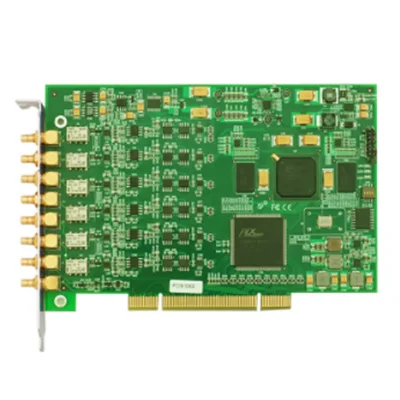
FPGA data acquisition card copy board
Name: FPGA data acquisition card copy board
Conversion precision: 14 bits
Output channel: 6 channels
Output range: ±2V, ±3V
Output Offset: Offset range up to ±2V, ±3V
Conversion rate: output frequency up to 2M/s
Calibration method: software automatic calibration
Storage space: 512MB, single channel not less than 70MB
Output impedance: < 1Ω
Trigger source: software trigger, external trigger
Trigger input signal: TRIG_IN
Standard TTL compatible: -0.5V ≤ low level ≤ 0.8V, 2.0V ≤ high level ≤ 5.5V
Trigger output signal: TRIG_OUT
Level range: low level ≤ 0.4V, high level ≥ 2
Pulse width: 1 sampling period (controlled by channel 0)
Trigger mode: single trigger, continuous trigger
Trigger direction: negative trigger, positive trigger, positive and negative trigger
Output interface: SMB (male)
What is a data acquisition card?
Data acquisition (DAQ) is the process of measuring events based on voltage, current, pressure, temperature, or sound. A DAQ system consists of high-speed data acquisition measurement hardware (DAQ cards or modules), input devices such as sensors, and a computer or processor.
What is an FPGA for data acquisition?
As the core of the data acquisition system, FPGA collects and stores data. The system is divided into three modules: front-end signal processing module, FPGA data acquisition module and data storage module. The FPGA data acquisition module is designed with VHDL and simulated by ISE software.
Name: FPGA data acquisition card copy board
Conversion precision: 14 bits
Output channel: 6 channels
Output range: ±2V, ±3V
Output Offset: Offset range up to ±2V, ±3V
Conversion rate: output frequency up to 2M/s
Calibration method: software automatic calibration
Storage space: 512MB, single channel not less than 70MB
Output impedance: < 1Ω
Trigger source: software trigger, external trigger
Trigger input signal: TRIG_IN
Standard TTL compatible: -0.5V ≤ low level ≤ 0.8V, 2.0V ≤ high level ≤ 5.5V
Trigger output signal: TRIG_OUT
Level range: low level ≤ 0.4V, high level ≥ 2
Pulse width: 1 sampling period (controlled by channel 0)
Trigger mode: single trigger, continuous trigger
Trigger direction: negative trigger, positive trigger, positive and negative trigger
Output interface: SMB (male)
