

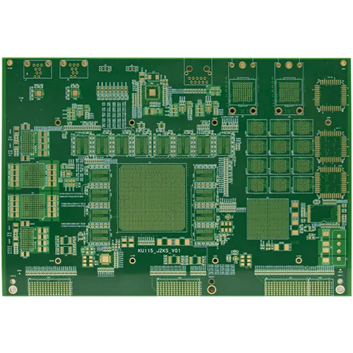
12-layer PCB circuit board
Name: 12-layer PCB circuit board
Layers: 12L
Sheet: FR4 Tg150
Plate thickness: 1.2mm
Panel size: 114*96mm/2
Outer copper thickness: 35μm
Inner layer copper thickness: 35μm
Minimum through hole: 0.20mm
Minimum BGA: 0.35mm
Line width line spacing: 3.8/3.8mil
Surface treatment: Immersion gold 2U''
Application field: RK3399 development board
12-layer PCBs provide the foundation for modern automotive electronic circuits. They play an important role in fast-tracking reliable interconnections. This PCB has a variety of uses, including navigation systems, transmission control units, electronic ignition assembly systems, and other components of the vehicle.
The 12-layer PCB is designed to withstand stressful conditions and high temperatures. The main material used here is polyimide. This polyimide material is organic in nature and has good heat resistance.
Gold is used by some of the top PCB manufacturers when finishing 12-layer PCBs. This is because it plays a huge role in resisting harsh environments. Additionally, some applications where heat sinks are added to ensure that the PCB operates at high temperatures dissolves easily.
Additionally, at 288 degrees Celsius and 20 seconds, the 12-layer PCB experiences thermal stress while its impedance is controlled around +/-10%. The cost of purchasing a 12-layer PCB is affordable compared to other multilayer boards such as 8-layer and 10-layer.
12-layer printed circuit boards can be used in the following areas:
Consumer Electronics
Computer Electronics
Telecom
Medical equipment
Aerospace and Military
Name: 12-layer PCB circuit board
Layers: 12L
Sheet: FR4 Tg150
Plate thickness: 1.2mm
Panel size: 114*96mm/2
Outer copper thickness: 35μm
Inner layer copper thickness: 35μm
Minimum through hole: 0.20mm
Minimum BGA: 0.35mm
Line width line spacing: 3.8/3.8mil
Surface treatment: Immersion gold 2U''
Application field: RK3399 development board
- Previous:Power Module PWB
- Next:14-layer PCB circuit board
