

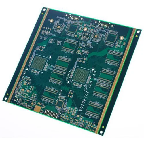
10-layer PCB circuit board
Name: 10-layer PCB circuit board
Layers: 10L
Sheet: FR4 Tg170
Plate thickness: 2.4mm
Panel size: 120*95mm/1
Outer copper thickness: 35μm
Inner layer copper thickness: 35μm
Minimum through hole: 0.20mm
Minimum BGA: 0.25mm
Line width line spacing: 3/3.2mil
Surface treatment: Immersion gold 2U''
Application field: network communication PCB board
10-layer PCB application
Preamplifiers, Satellite Antennas, GPS Tracking Devices, SAN Storage, AC Drives, GSM Signal Boosters, Mobile Broadband Routers, 220V Inverters, Memory Modules, Car Dashboards
10 Layer manufacturing process
Cut material to size/bake material —> Inner layer drilling —> Inner layer pattern transfer —> Inner layer circuit inspection —> Etch/stripping —> Etch inspection —> Browning —> Prepreg preparation —> Layers Pressing—> Cutting copper foil—> Positioning—> Laminating—> Target hole—> Drilling—> Desmear removal—> Immersion copper—> Image and text transfer—> Circuit inspection—> Copper and tin plating—> Film removal Etching—>Tin removal—>Etching inspection—> Dielectric inspection test—> Solder mask inspection—> Text—> Baking pan—> Spray tin, Immersion gold, Immersion tin—> Shape—> V cut— > Finished Product Test—> Antioxidant—> Final Inspection—> Finished Product Extraction—> Packaging
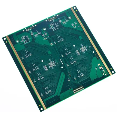
Name: 10-layer PCB circuit board
Layers: 10L
Sheet: FR4 Tg170
Plate thickness: 2.4mm
Panel size: 120*95mm/1
Outer copper thickness: 35μm
Inner layer copper thickness: 35μm
Minimum through hole: 0.20mm
Minimum BGA: 0.25mm
Line width line spacing: 3/3.2mil
Surface treatment: Immersion gold 2U''
Application field: network communication PCB board
- Previous:14-layer PCB circuit board
- Next:Medical Equipment PCB
