

10-layer communication switch PCB/PCBA design
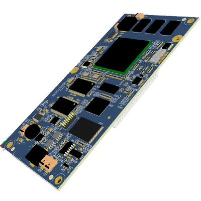
Name: 10-layer communication switch PCB/PCBA design
Sheet: IT180, F4BM, FR4, FR1-4, etc.
Designable layers: 1-32 layers
Minimum line width and line spacing: 3mil
Minimum laser aperture: 4mil
Minimum mechanical aperture: 8mil
Copper foil thickness: 18-175цm (standard: 18цm35цm70цm)
Peel strength: 1.25N/mm
Minimum punching hole diameter: single side: 0.9mm/35mil
Minimum hole diameter: 0.25mm/10mil
Aperture tolerance: ≤φ0.8mm±0.05mm
Hole tolerance: ±0.05mm
Hole wall copper thickness: double-sided/multi-layer: ≥2um/0.8mil
Hole resistance: double-sided/multi-layer: ≤300цΩ
Minimum line width: 0.127mm/5mil
Minimum pitch: 0.127mm/5mil
Surface treatment: rosin spray tin electric gold, anti-oxidation, chemical gold, carbon oil
Service: Provide OEM service
What is a communication switch?
A switched communication network transfers data from a source to a destination through a series of network nodes
Adaptive Communication Switch
Adaptive switches allow users with physical difficulties and special needs to activate assistive technology devices in their environment. Deceptively simple buttons, the right switch will open up access to a world of communications equipment, environmental controls, computer software and mobile devices.
Name: 10-layer communication switch PCB/PCBA design
Sheet: IT180, F4BM, FR4, FR1-4, etc.
Designable layers: 1-32 layers
Minimum line width and line spacing: 3mil
Minimum laser aperture: 4mil
Minimum mechanical aperture: 8mil
Copper foil thickness: 18-175цm (standard: 18цm35цm70цm)
Peel strength: 1.25N/mm
Minimum punching hole diameter: single side: 0.9mm/35mil
Minimum hole diameter: 0.25mm/10mil
Aperture tolerance: ≤φ0.8mm±0.05mm
Hole tolerance: ±0.05mm
Hole wall copper thickness: double-sided/multi-layer: ≥2um/0.8mil
Hole resistance: double-sided/multi-layer: ≤300цΩ
Minimum line width: 0.127mm/5mil
Minimum pitch: 0.127mm/5mil
Surface treatment: rosin spray tin electric gold, anti-oxidation, chemical gold, carbon oil
Service: Provide OEM service
