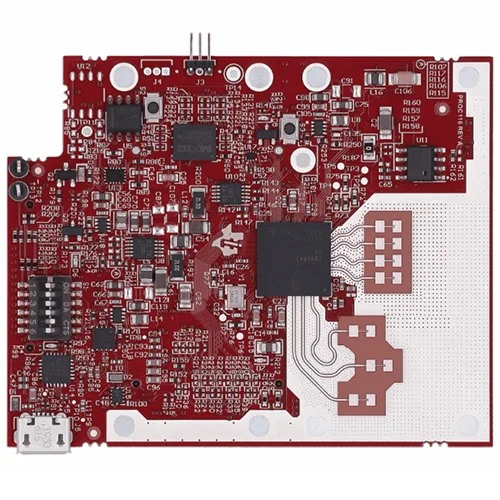
WARP Radio Hybrid PCB Assembly
Name: WARP Radio Hybrid PCB Assembly
Number of SMT lines: 7 high-speed SMT patch supporting production lines
SMT daily production capacity: more than 30 million points
Testing Equipment: X-RAY Tester, First Piece Tester, AOI AutomatIC Optical Tester, ICT Tester, BGA Rework Station
Placement speed: chip component placement speed (at best conditions) 0.036 S/piece
The smallest package that can be attached: 0201, the accuracy can reach ±0.04mm
Minimum device accuracy: PLCC, QFP, BGA, CSP and other devices can be mounted, and the pin spacing can reach ±0.04mm
IC type patch accuracy: it has a high level for mounting ultra-thin PCB boards, flexible PCB boards, gold fingers, etc. Can be mounted/inserted/mixed TFT display driver board, mobile phone motherboard, battery protection circuit and other difficult products
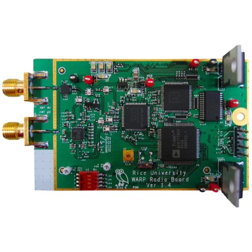
The WARP radio board utilizes a dual-band direct conversion radio transceiver from Maxim, the MAX2829. This transceiver supports both the 2.4 GHz and 5 GHz ISM bands. Although it is intended for use in 802.11a/b/g/n designs, this transceiver provides a flexible analog baseband interface. This interface allows the translation of any waveform, with a bandwidth up to 40 MHz, between baseband and RF, regardless of the waveform's adherence to an 802.11 standard. Further, when driven by a common reference clock, the phase coherency of the local oscillators in multiple MAX2829 transceivers is guaranteed. This feature is critical in MIMO applications as many algorithms require carefully controlled phase relationships and accurate measurements of phase among multiple antennas.
The WARP radio board's RF chain is completed by bandpass filters, a dual-band power amplifier and a Tx/Rx switch. The amplifier in the current design is capable of transmitting OFDM waveforms at 18 dBm. Future revisions of the board will likely incorporate more powerful amplifiers which will be better suited to long-range, outdoor deployment.
The WARP radio board is a 6-layer, 2x3" (4.5x7cm) PCB. The board houses all of the components necessary to provide a purely digital interface to the host board's FPGA. Dedicated linear power regulators are also used to meet the low noise requirements of the data converters and RF transceiver. The RF signals are routed to board-edge connectors to provide flexibility in the selection and arrangement of antennas.
Additionally, we provide hardware and software cores to enable the use of this daughtercard. The cores implement the details to control all devices on the board, allowing the user to call C functions to perform the various processes in a communications system.
Name: WARP Radio Hybrid PCB Assembly
Number of SMT lines: 7 high-speed SMT patch supporting production lines
SMT daily production capacity: more than 30 million points
Testing Equipment: X-RAY Tester, First Piece Tester, AOI AutomatIC Optical Tester, ICT Tester, BGA Rework Station
Placement speed: chip component placement speed (at best conditions) 0.036 S/piece
The smallest package that can be attached: 0201, the accuracy can reach ±0.04mm
Minimum device accuracy: PLCC, QFP, BGA, CSP and other devices can be mounted, and the pin spacing can reach ±0.04mm
IC type patch accuracy: it has a high level for mounting ultra-thin PCB boards, flexible PCB boards, gold fingers, etc. Can be mounted/inserted/mixed TFT display driver board, mobile phone motherboard, battery protection circuit and other difficult products
- Previous:No
- Next:mmWave Hybrid PCB Assembly